



Reduction and correction of sample surface charging effects in scanning electron microscopy imaging
Release time:
2024-02-18
Scanning electron microscopy (SEM) is a powerful imaging technique capable of providing high-resolution images of the sample surface. However, the charging effect on the sample surface often leads to image distortion and noise, which affects the imaging quality of the SEM. In this article, we will describe some common methods to reduce or correct the surface charging effect of the sample, thereby improving the accuracy and reliability of SEM imaging.
Scanning electron microscopy (SEM) is a powerful imaging technique capable of providing high-resolution images of the sample surface. However, the charging effect on the sample surface often leads to image distortion and noise, which affects the imaging quality of the SEM. In this article, we will describe some common methods to reduce or correct the surface charging effect of the sample, thereby improving the accuracy and reliability of SEM imaging.

This is usually the case for conductive samples. Therefore, when (η+δ) is 1, the measured Isc is zero
1. The use of conductive coatings In SEM imaging, the charging effect on the sample surface is mainly caused by the charge accumulation on the sample surface. To solve this problem, a thin layer of conductive electricity, such as metal or conductive carbon, can be applied to the surface of the sample. This conductive coating helps to create a conductive path on the surface of the sample, reducing the accumulation of surface charges.
Metallic coatings are a common choice because of their good conductivity and stability. Gold and platinum are commonly used metal coating materials because they are not volatile when subjected to electron beams. Methods of applying metal coatings include evaporation coating, sputtering coating, and electrochemical coating. These methods can be selected according to the shape and size of the sample to achieve a uniform coating.
In addition to metal coatings, conductive carbon materials can also be used to prepare conductive coatings. Conductive carbon materials have high electrical conductivity and good chemical stability, and are suitable for some samples that are sensitive to metals. Commonly used conductive carbon materials include graphene and carbon nanotubes. These materials can be applied to the surface of the sample by solution dispersion or direct deposition.
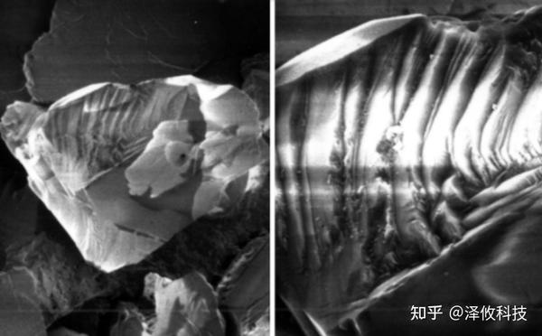
Example of negative charging effect on a diamond chip. At a low landing energy of 1 keV (HFW4 = 36 μm), the charging phenomenon is minimal (left figure). When the landing energy is increased to 10 keV (HFV = 13 μm), a strong charging phenomenon occurs (right figure)
Second, the use of metal conductive adhesive In some cases, the sample is not suitable for coating a thin layer of conductive conductivity, at this time, metal conductive adhesive can be used to reduce the charging effect. Metallic conductive adhesive is a special glue that contains metal particles that provide a conductive path. Applying a metal conductive adhesive to the surface of the sample or connecting the sample to the support substrate ensures that the charge can flow and reduces the effects of the charging effect.
The selection and application of metal conductive adhesives needs to consider the nature of the sample and the working conditions of the SEM. Some metal conductive adhesives have some adhesion to the sample and may affect the integrity of the sample. Therefore, when using metal conductive adhesives, it is necessary to choose the appropriate glue and take care to handle the sample gently during the operation to avoid sample damage.
3. Strategies for sample processing Sample processing is one of the important methods to reduce the charging effect. Treating samples in a vacuum or in an inert atmosphere can reduce oxidation and charge accumulation on the sample surface. This method requires the user to exercise caution in a laboratory environment to avoid contamination of the sample.
The specific method of sample handling depends on the material and nature of the sample. For example, for some samples that are susceptible to oxidation, heat treatment can be performed under vacuum conditions to remove the oxide layer from the sample surface. For some sensitive samples, it can be processed in an inert atmosphere to avoid chemical reactions in the sample.
4. Applications of low electron energy In SEM imaging, the interaction between the electron beam and the sample can lead to a charging effect. Imaging with low electron energies reduces the interaction between the electron beam and the sample, thereby reducing the effects of surface charging effects. However, this may reduce the resolution of the image.
In order to balance the charging effect and image resolution, the user can choose the appropriate electron energy based on the nature of the sample and the performance of the SEM. In some cases, the use of low electron energy can effectively reduce the charging effect, while in others, it may be necessary to increase the electron energy for better image resolution.
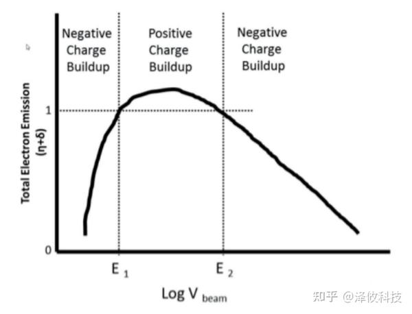
Total electron emission curve
5. Selection of Field Emission Electron Microscope Field emission electron microscopy is an advanced SEM technology, which can effectively reduce the charging effect. The stacked charge problem is less common in field emission electron microscopy because it uses field emitted electrons instead of an electron beam falling on the surface of the sample.
Field emission electron microscopy (FEM) has the advantages of high resolution and high contrast, making it suitable for imaging samples that are sensitive to the charging effect. However, FEM is more expensive and has more stringent requirements for the sample. Therefore, when using field emission electron microscopy, the choice needs to be based on the nature of the sample and the laboratory conditions.
6. Application of Electron Beam Suppressor Some advanced SEM equipment is equipped with electron beam suppressor, which can suppress the effect of electron beam and reduce the charging effect by applying a counterelectric field to the sample surface. The beam suppressor can be adjusted according to the nature of the sample and the operating conditions of the SEM to achieve the best suppression of the charging effect.
In SEM imaging, the charging effect on the sample surface is a common problem, resulting in image distortion and noise. To solve this problem, methods such as conductive coatings, metal conductive adhesives, sample handling, low electron energy, field emission electron microscopy, and electron beam suppressors can be used. The selection and application of these methods need to be considered based on the nature of the sample and the working conditions of the SEM to achieve the best imaging quality. Through the rational selection and application of these methods, the impact of charging effect can be reduced, and the accuracy and reliability of SEM imaging can be improved.

ZEPTOOLS ZEM18 Benchtop Scanning Electron Microscope
ZEPTOOLS is a scientific instrument company with fully independent intellectual property rights. Since the 1990s, our R&D team has been committed to providing excellent instruments for nanoscience research. At present, the company has a number of product lines including PicoFemto series of in-situ TEM measurement system, in-situ SEM measurement system, ZEM series of benchtop scanning electron microscope, JS series of step profiler, nano-displacement stage, two-dimensional material transfer stage, probe stage and cryogenic system, grating Ruler etc., which have gained a high degree of attention at home and abroad, and filled the gaps of the country's high-end precision instruments in the field of a number of blank.
Related News

Contact Us
Mobile Phone: 15756003283
Email: support@zeptools.com、micage@zeptools.com
Address: No.15, Electronic Venture Park, Dongshi, Tongling City, Anhui Province, China