



ZEPTOOLS:Detailed Analysis of Scanning Electron Microscope Electron Optics System
Release time:
2024-02-21
The electron optics system is the key to achieve high-resolution imaging in scanning electron microscopes (SEM). Its excellent design and optimization determines the instrument performance and image quality
The electron optics system is the key to achieve high-resolution imaging in scanning electron microscopes (SEM). Its excellent design and optimization determines the instrument performance and image quality. This article elaborates the composition, working principles and core technologies of the SEM electron optics system from aspects of electron gun, electromagnetic lens, aperture, scanning system and objective lens, analyzes the main difficulties and development trends, for readers to comprehensively and systematically understand the SEM electron optics system.
I. System Composition and Functions
The SEM electron optics system is responsible for providing a stable, high-intensity, well-shaped, controllable directional and zonal electron beam to meet the scanning needs of sample surfaces with different shapes, materials and potentials.

The system consists of electron gun, electromagnetic condenser lens, aperture, scanning system, stigmator and objective lens (Fig. 1). Each plays its own role and works together: the electron gun generates primary electron beam; condenser lens pre-focuses the beam; aperture filters out widely scattered electrons; scanning system drives the beam to scan over sample surface; stigmator corrects astigmatic aberrations; objective lens produces final fine focusing.
II. Electron Gun
The electron gun is the source that generates electron beam with determined energy. Its structure contains three electrodes: cathode (filament), grid and anode. SEM electron guns can be divided into three types by filament materials:
1、Tungsten hairpin filament
Tungsten releases electrons when heated to about 2100K. This utilizes the thermionic emission effect. But its large emission area leads to low current density, unable to produce very fine beam for high resolution. Advantage is low cost.

2、LaB6 electron gun
LaB6 emits higher density electron beam when heated to 1500-2000K. Compared with tungsten, LaB6 gun has higher brightness and smaller energy dispersion, achieves better resolution, but less market application.

3、Field emission electron gun
It uses single-crystal tungsten tip as cold emission source. Under high voltage, electrons emit through quantum tunneling effect. It has thermionic field emission with filament heating and cold field emission without heating. Cold field emission has highest resolution but worse stability. Thermionic field emission is preferred for SEMs.

III. Electromagnetic Condenser Lens
After generation, the electron beam needs to be focused by converging devices. Two main types are:
1、Electrostatic condenser lens
It focuses beams through the contour design of electric potential distribution between electrodes. Application is limited due to structure restrictions.

2、Magnetic condenser lens
More common one. It utilizes the Lorentz force acting on electrons passing through a magnetic field to bend trajectory and focus beams. Its typical structure consists of an iron-core coil with adjustable current to continuously tune the focusing power.

IV. Aperture
Aperture is often set between condenser lens and objective lens to remove widely scattered electrons, preventing them from impairing image quality. Under ideal conditions, only beams close to parallel with optical axis remain, forming smaller and more symmetric probe on sample surface, which is vital for high resolution.

Cleanliness and alignment of aperture also impact the results directly. Contaminations and deviations could block certain electrons, causing signal decline and quality reduction.

V. Scanning System
The scanning system drives the electron beam to scan over defined area on sample surface in a pre-programmed pattern, mapping images point-by-point. It consists of scan coils and scan signal generator. The generator outputs different frequencies, amplitudes and phases of X-Y signals. Scan coils accordingly generate electromagnetic fields to deflect beam tracks.
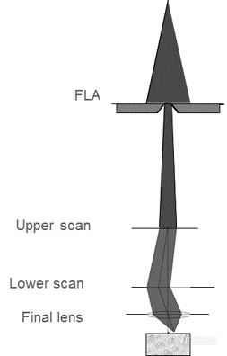
In the system, scan range is inversely related to magnification. Smaller range corresponds to larger magnification.
VI. Objective Lens
After the aperture, beam enters the objective lens part. It is a specially designed electromagnetic lens, responsible for the final accurate focusing and projection of electron probe onto sample fine structures.
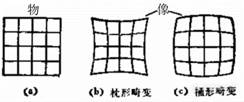
Varieties of objective lens designs exist, from early external placement to recent partial/full immersion modes, largely increasing resolutions by reducing spherical and chromatic aberrations. But the magnetic field also impairs observations on magnetic samples. Advanced SEMs now adopt switchable combined internal and external objective lens for both high resolution and versatility.
However, objective lens imaging still faces difficulties like diffraction limits, aberrations etc., which lead to larger beam spots. Different means must be taken such as tuning focus power, applying stigmator to achieve minimum probe size for optimum imaging.
VII. Development Trends
In summary, the maximum achievable SEM resolution highly relates to the probe size, which depends on the combined effects of brightness and monochromaticity of electron gun, abrasion control and objective lens design. Future resolution improvement lies in continuous optimization of electron sources for better parameters, synergistic system design to reduce aberrations, adaptive control and information technologies for autonomous compensation etc.

ZEPTOOLS ZEM18 Benchtop Scanning Electron Microscope
ZEPTOOLS is a scientific instrument company with fully independent intellectual property rights. Since the 1990s, our R&D team has been committed to providing excellent instruments for nanoscience research. At present, the company has a number of product lines including PicoFemto series of in-situ TEM measurement system, in-situ SEM measurement system, ZEM series of benchtop scanning electron microscope, JS series of step profiler, nano-displacement stage, two-dimensional material transfer stage, probe stage and cryogenic system, grating Ruler etc., which have gained a high degree of attention at home and abroad, and filled the gaps of the country's high-end precision instruments in the field of a number of blank.
Related News

Contact Us
Mobile Phone: 15756003283
Email: support@zeptools.com、micage@zeptools.com
Address: No.15, Electronic Venture Park, Dongshi, Tongling City, Anhui Province, China