



ZEPTOOLS - The Effect of Charge Effect in Scanning Electron Microscopy (SEM) Observation and Its Elimination
Release time:
2024-02-23
Scanning electron microscopy (SEM) is a powerful observation tool widely used in materials science, biology and other fields. However, the charge effect is a common and unpleasant phenomenon during SEM observation and can negatively affect image quality. In this article, we will introduce the formation principle of the charge effect, its effect on the image, and the effective methods to eliminate the charge effect.
Scanning electron microscopy (SEM) is a powerful observation tool widely used in materials science, biology and other fields. However, the charge effect is a common and unpleasant phenomenon during SEM observation and can negatively affect image quality. In this article, we will introduce the formation principle of the charge effect, its effect on the image, and the effective methods to eliminate the charge effect.
1. Formation of electric charge
According to the SEM principle introduced earlier, the electron beam continuously bombards the surface of the specimen, and only when the energy of the original electron beam is between V1 and V2, the secondary electron yield δ is 1, which means that the number of incident electrons and secondary electrons is equal, and the specimen does not absorb or release electrons, so no charge is formed. However, as long as the energy of the initial electron beam does not satisfy this condition, an absorbed current is formed to maintain the equilibrium of the charge, i.e., i0= ib+is+ia.
To achieve charge balance, the specimen needs to have good electrical conductivity. For conductors, this is no problem. However, for the sample that does not conduct electricity, or has poor conductivity and poor grounding, the excess charge cannot be conducted, and will accumulate on the surface of the sample, forming an electrostatic field, which affects the emission of the incident electron beam and secondary electrons, which is the charge effect.
Charge effects can have a range of effects on an image, including:
(1) Abnormal contrast: the emission of secondary electrons is irregularly affected, resulting in abnormal brightness or darkness in the image part;
(2) Image distortion: due to the electrostatic field generated by the charge, the incident electron beam is irregularly deflected, resulting in image distortion or stage difference;
(3) Image drift: The electrostatic field deflects the incident electron beam in a specific direction, resulting in image drift;
(4) Bright spots and bright lines: Irregular discharge often occurs in live samples, resulting in irregular bright spots and bright lines in the image;
(5) Image flatness and lack of three-dimensionality: It is usually due to the slow scanning speed and the long residence time of each pixel, which leads to the accumulation of charges, making the image look flat and lacking three-dimensionality.
Figure 1 illustrates a typical charge effect.

Fig.1 Typical charge effect
2. Elimination of charge
The generation of charge has a great influence on the observation of the SEM, so the normal SEM observation can only be carried out if the charge effect is eliminated or reduced. There are many ways to eliminate and reduce charge, but here are some commonly used:
First of all, it is necessary to pay attention to the sample preparation process in order to reduce the charge:
1) Reduce the sample size and minimize the contact resistance: this increases the conductivity of the specimen.
2) Coating treatment: The specimen is coated with a conductive film to improve its conductivity, which is also the most used method. There are two commonly used coating methods: evaporation and ion sputtering. Commonly used conductive films include gold (Au) and carbon. If you want to achieve better results, you can also use platinum (Pt), chromium (Cr), iridium (Ir), etc. The conductive film can not only effectively improve the conductivity, but also increase the secondary electron excitation rate. The film thickness is now relatively easy to control, and there is no effect on the specimen topography within a certain magnification range.
However, the coating also has its drawbacks, such as the coating will be covered by a film layer after coating, which will affect the true topography of the sample. In severe cases, it can also produce artifacts, which will have a great impact on some ultra-high-resolution observations or the measurement of some details (such as pores and fibers), as well as EDS and EBSD analysis.
As shown in Figure 2, graphite is coated with a platinum film to create an artifact. As shown in Figure 3, the fibers are coated with a metal film, resulting in a microscopic coarsness and smaller pores.
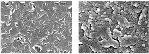
Fig.2. Artifacts after graphite gold plating
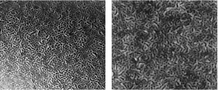
Fig.3 Image of the fiber before (left) and after (right) gilding
In addition to sample preparation, it is also necessary to find suitable EM working conditions as much as possible to eliminate or reduce the effects of charge:
3) Reduce the beam current: Reducing the intensity of the incident electron beam can reduce the accumulation of charge.
4) Reduce the magnification: Use a low magnification observation as much as possible, because the larger the magnification, the smaller the scanning range, and the faster the charge accumulates.
5) Faster scanning: The electron beam stays in the same area for a long time, which can easily cause charge accumulation. At this point, the scanning speed of the electron beam can be accelerated, and the dwell time in different areas can be shortened to reduce the charge effect.
6) Change the image acquisition strategy: When the scanning speed is accelerated, the signal-to-noise ratio of the image will be greatly reduced. In this case, line accumulation or frame superposition averaging can be used to reduce the charge effect and improve the signal-to-noise ratio. Line accumulation has a good suppression effect on slight charges, while frame overlay has a good suppression effect on high noise generated by fast sweeps. However, the image must not have drift, otherwise it will create ghosting and cause the image to be blurry.
As shown in Figure 4, the sample is a polymer sphere. When the scanning speed is slow, the specimen is easily damaged and deformed, but with the acquisition method of fast scanning and line accumulation at the same time, the specimen is intact and the image still has a good signal-to-noise ratio.

Fig.4. Comparison of polymer spherical samples under different scanning methods
7) Reducing voltage: Reducing the energy of the incident electron beam (to within V2) can also effectively reduce the charge effect. As shown in Figure 5, the specimen is a polystyrene ball, which has obvious charge phenomenon at the acceleration voltage of 5 kV, but when the accelerating voltage is reduced to 2 kV, the charge effect is basically eliminated. However, as the accelerating voltage decreases, there are also side effects of reduced resolution.
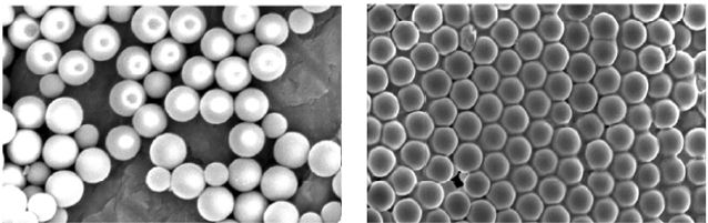
Figure 5 Reducing the acceleration voltage to eliminate the effect of charge
8) Use a secondary electron detector or backscattered electron detector in a non-mirror tube for observation: when a large amount of charge is generated, many secondary electrons will be pushed upward, resulting in too many electronic signals received by the secondary electron detector in the lens tube, resulting in a charge effect, especially in the immersion mode. In this case, the use of a detector outside the pole shoe, which receives a relatively small amount of electronic signal, can reduce the charge effect, as shown in Figure 6. In addition, the energy of the backscattered electrons is higher, and the yield and exit direction are much less affected by the charge than the secondary electrons, so the observation of the backscattered electron image can also effectively reduce the charge effect, as shown in Figure 7, showing the comparison of the alumina template in the secondary electron and backscattered electron images.
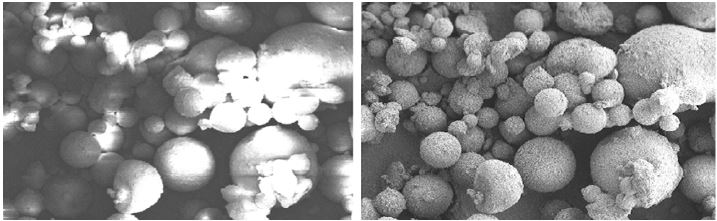
Fig.6. Effect of detectors inside the lens tube (left) and outside the lens tube (right) on the charge
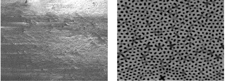
Fig.7 Effect of SE (left) and BSE (right) images on charge
9) Tilt the sample: Tilting the sample to a certain angle can increase the yield of secondary electrons on the surface of the sample, thereby weakening the effect of the charge effect.
In addition to the methods described above, electron microscope manufacturers are developing new techniques to reduce or eliminate charging effects, the most common of which is low-vacuum technology. Low vacuum technology is a very effective means of removing the charge of the specimen, but it needs to be equipped with the electron microscope itself.
10) Low Vacuum Mode: In low vacuum mode, the ionization of ions or gas molecules is used to neutralize the generated charge, thereby eliminating the charge effect under electron microscopy conditions that do not require the coating of conductive films or the use of strict conditions. However, in low vacuum, the original electron beam is scattered by gas molecules, which results in some degradation in terms of resolution, signal-to-noise ratio, and contrast. As shown in Figure 8, the charge-free effect of secondary electrons and backscattered electrons can be observed on biological samples without coating with a conductive film.

Fig.8. Comparison of the effects of low-vacuum BSE (left) and SE (right).
Considering the properties of the specimen, the observation requirements and the technical conditions of the electron microscope, the appropriate method can be selected to eliminate or reduce the charge effect to obtain clear and accurate SEM images. The understanding of the charge effect and its corresponding solutions will help to improve the effectiveness and accuracy of SEM observations, and promote research and application in related fields.

ZEPTOOLS ZEM20 Benchtop Scanning Electron Microscope
ZEPTOOLS is a scientific instrument company with fully independent intellectual property rights. Since the 1990s, our R&D team has been committed to providing excellent instruments for nanoscience research. At present, the company has a number of product lines including PicoFemto series of in-situ TEM measurement system, in-situ SEM measurement system, ZEM series of benchtop scanning electron microscope, JS series of step profiler, nano-displacement stage, two-dimensional material transfer stage, probe stage and cryogenic system, grating Ruler etc., which have gained a high degree of attention at home and abroad, and filled the gaps of the country's high-end precision instruments in the field of a number of blank.
Related News

Contact Us
Mobile Phone: 15756003283
Email: support@zeptools.com、micage@zeptools.com
Address: No.15, Electronic Venture Park, Dongshi, Tongling City, Anhui Province, China