



What is a step gauge? What is the working principle of a step gauge?
Release time:
2025-08-06
A profilometer is a precision instrument used for high-precision measurement of the microscopic topography of material surfaces (such as step height, roughness, flatness, and warp). It is widely used in semiconductor manufacturing, materials science research, MEMS (Microelectromechanical Systems) processing, and optical component testing. Its core function is to obtain quantitative data on surface height changes through minute contact between the probe and the sample surface, providing key data for material performance analysis and process optimization.
I. What is a Step Profiler?
A step profiler (Profilometer) is a precision instrument used for high-precision measurement of the microscopic topography of material surfaces (such as step height, roughness, flatness, warping, etc.). It is widely used in semiconductor manufacturing, materials science research, MEMS (Microelectromechanical Systems) processing, optical component testing, and other fields. Its core function is to obtain quantitative data on surface height changes through the minute contact of a probe with the sample surface, providing key data for material performance analysis and process optimization.
II. Working Principle of a Step Profiler
The core principle of a step profiler is based on "probe contact scanning + sensor feedback" technology. The specific process is as follows:
Probe Surface Contact An extremely fine, hard probe (radius of curvature usually ≤2μm) is used to contact the sample surface with an extremely light force (0.5~50mg), similar to "lightly stroking" across the area to be measured, avoiding damage to the sample.
Scanning and Data Acquisition Through uniform movement of the sample stage or probe in the X-Y plane, the instrument records the Z-axis (height) data of all points on each line scanned by the probe; after splicing the height data of multiple scan lines, a dense "height array" is formed.
Sensor Feedback and Calculation :
- Force Control An LVDT (Linear Variable Differential Transformer) sensor detects the deformation of the spring, precisely controlling the pressure applied by the probe (constant force control) to ensure measurement consistency.
- Displacement Measurement A piezoelectric ceramic drives the micro-stage to produce displacement (travel ≥1mm), and the micro-stage LVDT sensor provides real-time feedback on displacement changes. This displacement is the step height of the measured area.
3D Topography Rendering The software processes the height array data and renders it into a 3D topography map, visually displaying microscopic surface features (such as step edges, scratches, and protrusions).
III. Zeo Technology Step Profiler: "Made in China" High-Precision Measurement—JS Series Technology Analysis and Advantages
In the fields of semiconductors and precision material testing, high-precision and high-stability step profilers are key tools for measuring process levels. As a leading domestic manufacturer of precision measurement equipment, Dongguan Zeo Technology Co., Ltd. (hereinafter referred to as "Zeo Technology") launched the JS series step profilers (including manual, semi-automatic, and fully automatic models), with core technological breakthroughs and flexible upgrade capabilities, are becoming a benchmark for high-end domestic measurement equipment.
(1) Product Matrix: "Customized" Solutions Covering All Scenarios
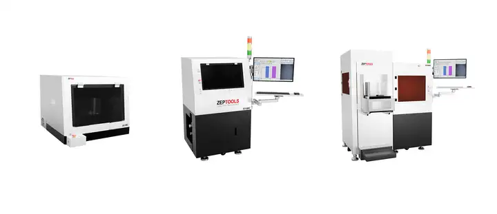
The Zeo JSC series has created a three-tier product system for different users' testing efficiency and sample size requirements:
- Manual Type (JS 10C) Suitable for small-batch testing in laboratories, supporting manual control of horizontal (X/Y) and rotational (RZ) axes, sample thickness ≤50mm, maximum scan length 55mm, vertical resolution up to 0.05nm (full scale), and repeatability deviation ≤0.5nm (30 scans of a 10μm standard block).
- Semi-automatic Type (JS 100C/200C/300C) Suitable for medium-batch testing, with electric control of the sample stage X/Y/Z axes, supporting ±360° high-precision rotation (0.1° resolution), sample sizes covering 6 inches to 12 inches, host weight 350~460kg, balancing efficiency and stability.
- Fully Automatic Type (JS 2000C/3000C) For large-scale production line testing, integrated image recognition system (positioning accuracy ±10μm), supporting single scan ≤55mm, wafer thickness ≤50mm, production efficiency ≥10 pieces/hour (single-side measurement ≥5 positions), meeting the needs of semiconductor wafer mass production testing.
(2) Core Technology: Dual LVDT Sensors + Modular Design, Defining a New Benchmark for Domestic Precision
The technological advantages of the Zeo JSC series stem from two core innovations:
Dual LVDT Sensor "Double Insurance" :
- Sensor LVDT: Real-time detection of spring deformation, precisely calculating the pressure applied by the probe (0.5~50mg), ensuring safe measurement of soft/brittle materials (such as silicon, lithium tantalate, glass).
- Micro-stage LVDT: Feedbacks piezoelectric ceramic displacement, directly outputting step height data, with a vertical resolution of 0.05nm and repeatability error ≤0.5nm (comparable to international first-line products).
- This design avoids the defects of traditional capacitive sensors being easily affected by the environment, greatly improving measurement reliability.
Modular Upgrades, Protecting User Long-Term Investment :
The Zeo JS series supports "low-cost upgrades": upgrading from the early JSB series to the JSC series only requires replacing parts such as the coarse adjustment stage, sample lifting stage, and marble base, and updating the software driver; existing JS models can later be directly compatible with a 1mm range (original maximum 80μm) by replacing the probe components, flexibly adapting to new material testing needs.
(3) Competitor Comparison: Dual Advantages of Performance and Cost-Effectiveness
Compared with international brands such as Bruker Dektak XT and KLA P-7, the Zeo JSC series achieves "parity or even surpasses" in core indicators:
- Measurement Accuracy Vertical resolution 0.05nm (on par with Bruker Dektak XT), repeatability ≤0.5nm (better than some competitors).
- Functional Coverage Supports multi-parameter measurements such as steps, roughness, flatness, and warping, with standard dual cameras (main camera 115x + auxiliary camera for real-time observation), making operation more convenient.
- Localized Service As a domestic manufacturer, Zeo Technology provides faster delivery times, more flexible customized solutions (such as optional floor-standing/desktop air-floating tables), and after-sales response, reducing the overall cost for users.
(IV) Application Scenarios: A "Versatile Player" from the Lab to the Production Line
Thanks to its high precision and stability, the ZEPTOOLS JS series has been widely used in:
- Semiconductor Manufacturing : Wafer surface step height detection, thin film deposition uniformity analysis;
- Materials Science : Surface morphology characterization of nanomaterials and MEMS devices;
- Optical Processing : Surface roughness and warp measurement of precision components.
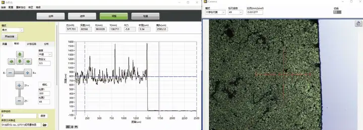
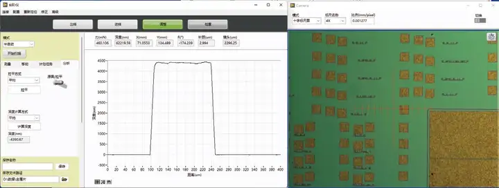
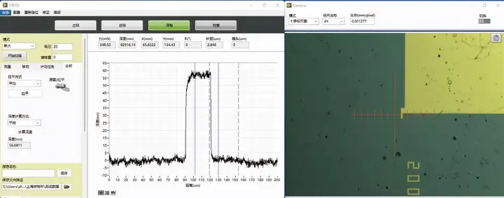
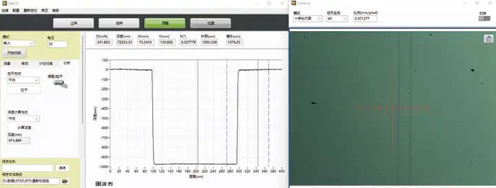
Choose ZEPTOOLS JS, Choose "Chinese Precision"
Against the backdrop of the rise of high-end domestic instruments, ZEPTOOLS Technology's JSC series of step profilers, with its core technology of independent innovation, flexible upgrade solutions, and localized services, provides a reliable "Made in China" choice for the semiconductor and materials fields. Whether it's basic research in the laboratory or large-scale testing on the production line, the ZEPTOOLS JSC series will assist users in breaking through technological bottlenecks and seizing market opportunities with its "0.05nm-level" precision.
Related News

Contact Us
Mobile Phone: 15756003283
Email: support@zeptools.com、micage@zeptools.com
Address: No.15, Electronic Venture Park, Dongshi, Tongling City, Anhui Province, China