



What is maskless lithography? How does it work?
Release time:
2025-08-06
Maskless lithography is an advanced lithography equipment that does not require a physical mask. It uses a digital micromirror device (DMD) to dynamically generate lithographic patterns, enabling flexible and efficient micro-scale structure processing. Its core function is utilizing the spatial light modulation capability of the DMD to directly project computer-designed patterns onto the substrate surface. This eliminates the cumbersome steps of mask making and alignment in traditional lithography, significantly shortening the R&D cycle and reducing production costs.
I. What is maskless lithography?
Maskless lithography is an advanced lithography equipment that does not require a physical mask. It uses a digital micromirror device (DMD) to dynamically generate lithographic patterns, enabling flexible and efficient micro-scale structure processing. Its core lies in utilizing the spatial light modulation capability of the DMD to directly project computer-designed patterns onto the substrate surface, eliminating the cumbersome steps of mask making and alignment in traditional lithography, significantly shortening the R&D cycle and reducing production costs.
II. Working Principle and Technological Breakthroughs
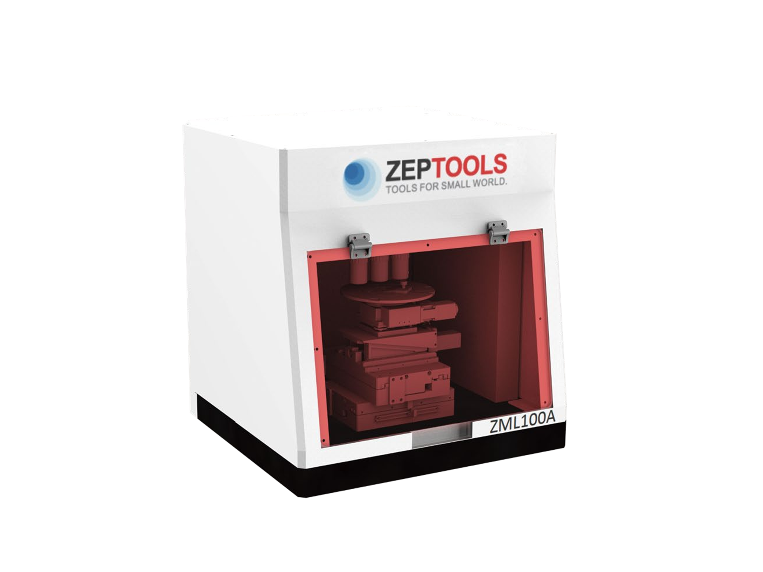
ZEPTOOLS Technology's ZML series of maskless lithography machines use the following core technologies:
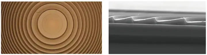
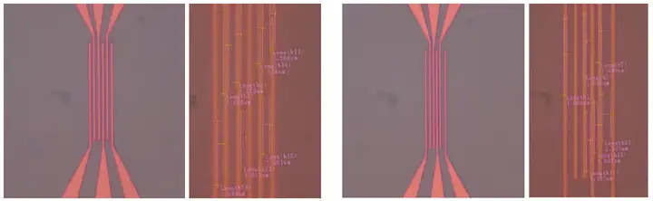
1. DMD Dynamic Projection By modulating ultraviolet light (405nm) using millions of programmable micromirror units (each measuring only 7.6μm), the digital pattern is projected in real-time onto the sample surface. It supports 8-bit grayscale lithography, precisely controlling light intensity distribution to achieve one-step molding of three-dimensional microstructures.
2. High-Precision Motion System
Linear motor displacement stage Repetitive positioning accuracy ±0.25μm, supporting large-area stitching lithography of 100×100mm
Electrically driven leveling rotary stage Pitch and tilt adjustment accuracy 1.85°/revolution, compatible with 4/8-inch wafers
Laser active focusing Real-time monitoring of focal plane offset to ensure multilayer overlay accuracy of ±0.5μm
3. High-Precision Motion System
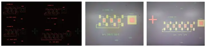
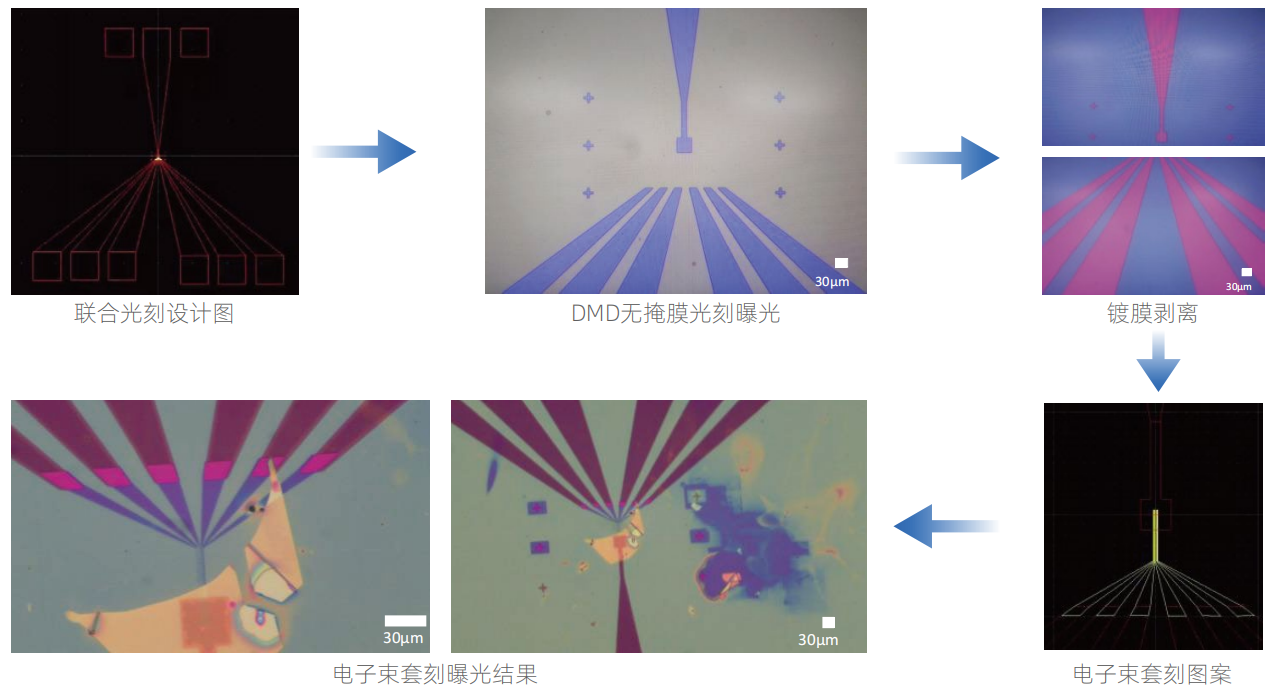
Supports DXF/GDS/BMP format import, automatically generating exposure paths
The overlay guidance system automatically calculates rotation/translation parameters through cross markers
The in-situ drawing function allows direct annotation and modification of the design on the microscope screen
III. Core Advantages Compared to Traditional Lithography
| Dimension | Traditional Mask Lithography | ZEPTOOLS DMD Maskless Lithography |
|---|---|---|
| Mask Cost | High (hundreds of thousands to millions of RMB) | Zero (digital storage, unlimited reuse) |
| Pattern Modification Cycle | 3-7 days (requires remaking the plate) | Real-time modification, effective in seconds |
| Minimum Line Width | ≥1μm (limited by photoresist) | 0.5μm (optical limit) |
| Gray Scale Control | Binary (on/off) | 256 levels of grayscale (continuous morphology control) |
| Applicable Scenarios | Mass standardized production | Rapid prototyping, MEMS, personalized customization |
IV. Typical Application Scenarios
1. MEMS Device Manufacturing
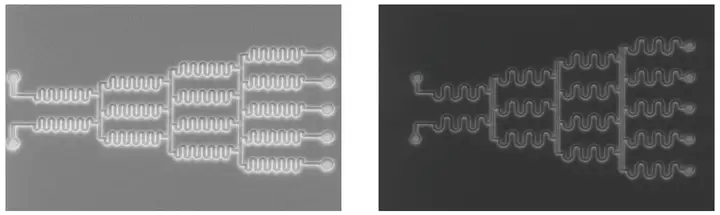
Piezoelectric micromirror array (feature size 30μm)
Microfluidic chip (channel depth 10μm, stitching accuracy ±0.3μm)
2. New Material Research and Development
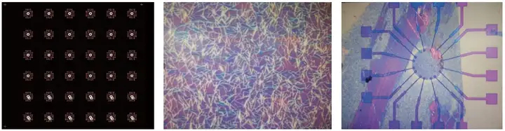
Tellurium nanogrid electrode (30nm step continuity verification)
Two-dimensional material transfer (Ti/Au/Ti layered thickness 12nm)
3. Scientific Research and Education
Rapid preparation of test structures in university laboratories
Prototype verification in research institutes (supports 8-inch wafer compatibility)
V. ZEPTOOLS Technology's Technological Leadership
As a leading domestic enterprise in DMD lithography technology, ZEPTOOLS Technology continues to promote domestic substitution:
Patent Barriers Possesses independently owned intellectual property rights for grayscale algorithms and stitching accuracy compensation technology
Full-Chain Integration Vertical integration from light source optimization (405nm high uniformity LED array) to motion control (±0.25μm repeatability)
Ecosystem Construction Equipped with ZEPTOOLS software to realize full-process management from design to mass production
VI. Industry Value
The launch of ZEPTOOLS's maskless lithography machine has enabled Chinese enterprises to achieve key technological breakthroughs in the following areas:
Cost Revolution The cost of single exposure is reduced to 1/10 of the traditional method
Agile Manufacturing Sample delivery cycle is compressed from weeks to hours
Innovation Empowerment Provides underlying support for emerging sectors such as medical MEMS and flexible electronics
Official Website :www.zeptools.cn
Technical Support : support@zeptools.com
National Service Network :Shanghai, Beijing, Dongguan, and Tongling Centers
Inquire Now :Get a free sample testing plan to accelerate your micro-nano innovation!
Keywords: Maskless Lithography/DMD Lithography Technology/MEMS Manufacturing/Microfluidic Chip/Domestic Substitution/Gray-scale Lithography/Precision Machining Equipment/Domestication of Semiconductor Equipment
Related News

Contact Us
Mobile Phone: 15756003283
Email: support@zeptools.com、micage@zeptools.com
Address: No.15, Electronic Venture Park, Dongshi, Tongling City, Anhui Province, China