



What is the working principle of an electron beam lithography machine?
Release time:
2025-08-06
Electron beam lithography (EBL) is a micro-nano fabrication device based on electron beam exposure. Its core principle is to draw nano-scale patterns on a resist (such as PMMA, HSQ) using a high-energy electron beam. Finally, the pattern is transferred to the substrate material through processes such as development and fixing.
I. Working Principle of Electron Beam Lithography
Electron beam lithography (EBL) is a micro-nano fabrication device based on electron beam exposure. Its core principle is to use a high-energy electron beam to draw nano-scale patterns on a resist (such as PMMA, HSQ). Finally, through development, fixing and other processes, the pattern is transferred to the substrate material. The following are its key workflows and technical logic:
1. Electron Beam Generation and Focusing
The core component of an electron beam lithography system is the electron gun (such as the Schottky field emission electron gun used in ZEL304G). A high-voltage power supply (acceleration voltage 20V~30kV) excites the electron source to emit a high-brightness, low-divergence electron beam. The electron beam is focused by a condenser lens and an objective lens to form an extremely fine beam spot with a diameter ≤2nm, ensuring high pattern resolution (≤1nm@15kV).
2. Pattern Scanning and Exposure
The focused electron beam is controlled by a pattern generator, which drives the beam deflector through a D/A deflection amplifier, performing vector scanning according to the preset graphic path (such as DXF/GDS files). (Supports sequential scanning, cyclic scanning, spiral scanning, and other modes). During scanning, the electron beam only writes in areas where the pattern exists (vector scanning advantage), avoiding energy loss in ineffective areas and improving efficiency.
3. High-Precision Positioning and Stitching
The sample stage is the key to achieving precise preparation of micro-nano structures. The ZEL304G is equipped with a standard laser interferometer sample stage with a travel range ≤105mm. It uses laser interferometry to monitor the sample position in real time, achieving sub-nanometer positioning accuracy. It supports large-stroke high-precision stitching (such as seamless stitching of long gratings) and multi-layer overlay (calibrating the position using a two-point calibration function without pre-marking).
4. Pattern Optimization and Correction
To solve the electron beam proximity effect (pattern distortion caused by electron scattering in adjacent areas), the equipment has a built-in proximity effect correction function, which optimizes the dose distribution through HeatMap analysis; it also supports dose correction (customizing the exposure dose of different patterns) to ensure ultra-fine structures at the 0.38nm level in minimum linewidth tests (such as the exposure results of a design model groove width of 200nm).
5. Resist Processing and Pattern Transfer
After exposure, the resist needs to undergo development (e.g., PMMA uses MIBK:IPA=1:3 strong developer or IPA weak developer), fixing, and other processes to finally transfer the electron beam-written pattern to the substrate (such as silicon wafer, silicon dioxide), forming micro-nano structures (such as quantum devices, MEMS, metasurfaces, etc.).
II. ZepTools: Defining New Benchmarks in Micro-Nano Fabrication Through Independent Innovation—Technological Breakthroughs and Application Empowerment of Electron Beam Lithography
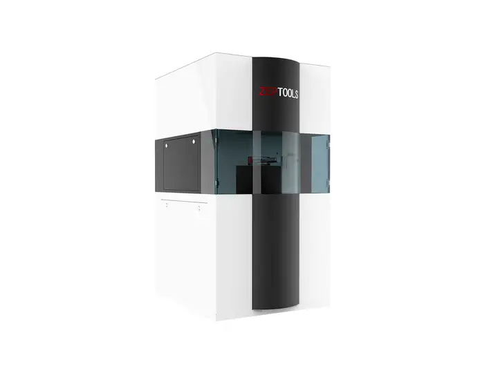
In the global semiconductor and micro-nano manufacturing fields, the precision of micro-nano structures directly determines device performance. As a leading enterprise in advanced equipment manufacturing in China, ZepTools, with 20 years of technological accumulation and independent innovation capabilities, has launched the ZEL304G, ZEL204W, and other series of electron beam lithography systems. With "high resolution, high precision, and high compatibility" as its core advantages, it has become the preferred partner for research institutions and industrial fields to break through the bottlenecks of micro-nano processing.
(I) Core Technology: "Full-Chain High-Precision and High-End" from Electron Gun to Sample Stage
The core competitiveness of ZepTools electron beam lithography systems comes from its in-depth independent research and development of key components. Taking the flagship model ZEL304G as an example:
Field Emission Electron Gun :Uses Schottky field emission technology, with high electron beam brightness and a small divergence angle. Combined with a wide range of acceleration voltages from 20V to 30kV (1kV steps), it achieves ultra-high resolution of ≤1nm@15kV, meeting the needs of extreme scenarios such as minimum linewidth testing and metasurface preparation.
Laser Interferometer Sample Stage :Standard configuration with a high-precision platform with a travel range ≤105mm. It uses laser interferometry to track the sample position in real time, achieving sub-nanometer positioning accuracy. It supports large-stroke stitching (such as 50μm writing field stitching of a 100μm × 100μm cross pattern) and multi-layer overlay, with errors controllable at the nanometer level.
High-Performance Pattern Generator :Equipped with a 20-bit D/A converter and a 50MHz high-speed scanning module, it supports multiple scanning modes such as sequential, cyclic, and spiral scanning. Combined with the FPGA control core, it achieves a balance between high-speed scanning and ultra-high resolution, with a minimum linewidth of 2nm for a single exposure.
(II) Full-Process Control: "Zero-Error" Guarantee from Design to Mass Production
ZepTools electron beam lithography systems are not only top-of-the-line in hardware but also achieve precise control of the entire process through an intelligent software system:
Exposure Software V1.0.5.3 :Supports importing mainstream formats such as DXF/GDS/BMP. It allows customization of exposure dose and scanning path (Z-type, S-type, etc.), and provides features such as "field stitching" and "overlay." For example, using the "two-point calibration" technology, calibration of the exposure position can be achieved on substrate feature points (such as impurities) without pre-marking, achieving ±0.1μm overlay accuracy; the "dose correction" function optimizes the influence of electron scattering through HeatMap analysis to ensure the sharpness of the edges of complex patterns.
Resist Process Adaptability :Compatible with various resist materials such as PMMA (positive) and HSQ (negative), supporting thick resist testing and different pre-baking conditions (such as 180℃ baking for 2min), covering all scenarios from low-resolution large-area patterns to high-resolution small linewidths (0.38nm).
(III) Application Empowerment: "Two-Way Rush" for Research and Industry
The application scenarios of ZepTools electron beam lithography systems have extended to cutting-edge fields such as semiconductors, quantum research, MEMS, and photonic crystals:
Research Field :Provides solutions such as uniformity testing and seamless stitching of long gratings (304nm period) for universities and research institutions, assisting in breakthroughs in basic research such as quantum tunneling devices and three-dimensional metasurfaces.
Industrial Field :Supports mass production needs such as microelectromechanical system (MEMS) processing and photolithography mask manufacturing. Through high-precision stitching and overlay functions, it improves production efficiency and yield.
In an era where micro-nano manufacturing is moving towards "smaller, finer, and more complex," ZEPTOOLS Technology, with its electron beam lithography machine at its core, leverages its independently innovative core technologies, full-process high-precision control capabilities, and application scenarios covering scientific research and industry to continuously create value for customers. In the future, ZEPTOOLS Technology will continue to cultivate the micro-nano manufacturing field, driving industrial upgrades through technological breakthroughs and helping global customers seize new heights in the micro-nano technology competition!
Related News

Contact Us
Mobile Phone: 15756003283
Email: support@zeptools.com、micage@zeptools.com
Address: No.15, Electronic Venture Park, Dongshi, Tongling City, Anhui Province, China