



ZEPTOOLS Technology Popular Science - Introduction to Electron Beam Lithography (EBL) Technology
Release time:
2025-08-07
Electron beam lithography (EBL) is a maskless, direct-write lithographic technique that works by directly writing nanoscale patterns onto an electron-sensitive resist surface using a focused electron beam.
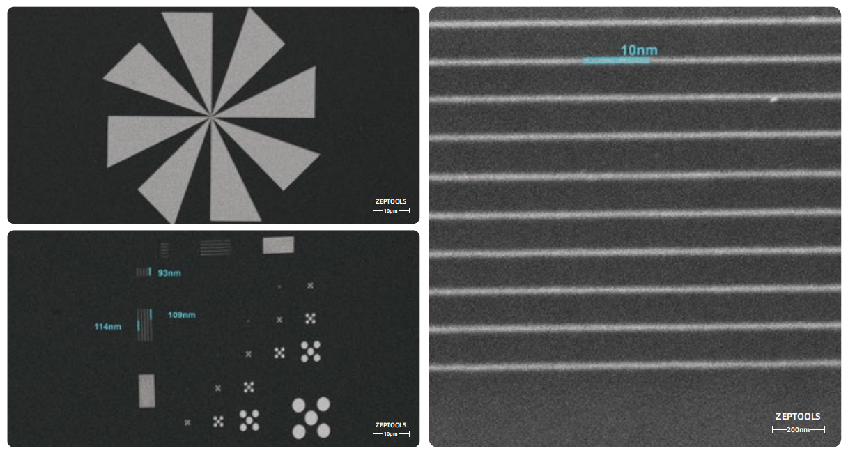
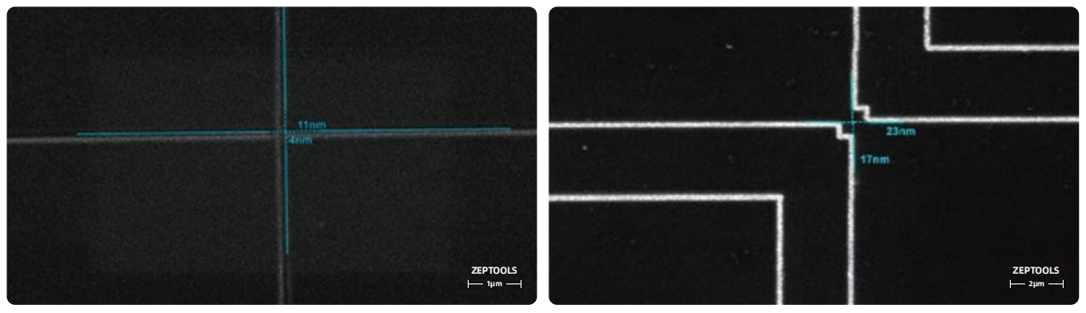
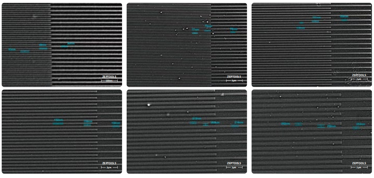
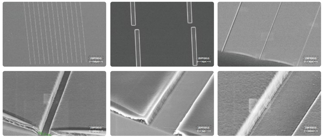
Electron beam lithography (EBL) is a direct-write lithography technique that does not require a mask. It works by directly writing nanoscale patterns on the surface of an electron-sensitive resist using a focused electron beam. This technology has two significant advantages: firstly, it has ultra-high resolution (achieving a minimum feature size of <10nm), and secondly, it supports flexible maskless pattern design. However, due to limitations such as low exposure efficiency and complex system control, electron beam lithography is currently mainly used in three areas: the fabrication of lithographic masks, the development of advanced prototype devices, and nanoscale scientific research and device development. This technology is particularly suitable for small-batch, high-precision micro-nano structure processing needs.
Development History
The development history of electron beam lithography (EBL) can be traced back to the early 20th century, to the origins of focused electron beam technology. Its technological evolution is almost synchronized with optical lithography, but the two ultimately formed a complementary and coexisting pattern.
Technical Prototype Stage
Early focused electron beam technology was applied to cathode ray tube (CRT) displays, while the advent of the scanning electron microscope (SEM) in the 1960s laid the basic structural framework for electron beam exposure systems. However, true electron beam lithography technology began with the development of electron beam sensitive resists.
Key Breakthrough Period (1950s–1970s)
1958: Researchers at MIT first used electron-induced carbon contamination to form an etching mask, achieving the preparation of high-resolution two-dimensional graphics.
1965: Electron beam exposure technology broke through the 100nm structure processing barrier.
1968: PMMA was established as an electron beam resist, significantly promoting the improvement of graphic accuracy.
1970: A 0.15μm surface acoustic wave device was fabricated using PMMA.
1972: 60nm × 60nm cross-sectional aluminum metal lines were processed on a silicon surface.
In the 1980s, electron beam lithography was once considered an alternative to optical lithography, but due to its inherent limitations of low exposure efficiency and high cost, it ultimately failed to replace optical lithography. After decades of development, the two have formed a clear division of labor: electron beam lithography focuses on mask preparation, nanoscale research prototype development, and small-batch high-precision processing, while optical lithography dominates large-scale integrated circuit production.
Theoretical Basis
The core principle of lithography technology is to utilize light irradiation to cause changes in a polymer, thereby forming the desired pattern. In optical exposure, the resolution is significantly limited by the wavelength of light. In order to break through this limitation and improve resolution, the selection of light waves has undergone a continuous shortening development process, from the initial G-line and I-line, gradually developing to deep ultraviolet, and now to extreme ultraviolet.
Electron beams are essentially charged particles. According to the wave-particle duality theory, their wavelength can be calculated using a specific formula. From this, it can be known that the higher the accelerating voltage of the electron beam, the smaller the corresponding electron beam wavelength, and this characteristic is directly related to whether the electron beam exposure system is a high-voltage system or a low-voltage system. For example, in a 100KV accelerating voltage system, the electron wavelength is only 0.12nm, which is the basic guarantee for electron beam lithography to achieve high resolution. However, traditional electron beam lithography uses a direct-write mode, which is a major reason for the low efficiency of current electron beam lithography, but it also has significant advantages—the direct-write process does not require a mask, the operation is simple and flexible.
Like ultraviolet light, electron beams can also cause chemical bond breakage or crosslinking reactions in some polymers, thereby forming corresponding patterns during development. Even some ultraviolet photoresists can be used as electron beam resists, so there is not much difference in essence between the two. To distinguish them, we sometimes refer to electron beam resists as resists. However, because electron beams produce scattering when interacting with matter, their interaction process is much more complex than ultraviolet lithography.
Electron Beam Exposure System
Electron beam lithography technology originated from scanning electron microscopy. It is a graphic transfer technology based on the principle of focused electron beam scanning.
The composition of an electron beam lithography system is relatively complex, mainly including 3 basic components and several auxiliary components. Among them, the basic components are the electron gun, electron lens, and electron deflector; auxiliary components include the vacuum system, workpiece stage control system, etc.
The role of the electron gun is to produce controllable and focused electrons. Depending on the working method, it is usually divided into thermionic sources and field emission sources. The working principle of the thermionic source is to heat the cathode to a sufficiently high temperature so that the electrons in the cathode material obtain sufficient kinetic energy to break through the potential barrier of the electron gun metal work function and be emitted, forming an electron beam. The field emission source, on the other hand, uses a strengthened electric field to allow electrons to tunnel through the potential barrier to form an electron source.
The electron beam emitted from the electron emission source is focused and deflected in the electron column. The electron column consists of a series of electron lenses, apertures, baffles, etc. Specifically, the electrons are first shaped by the aperture, then converged into a spot by the electron lens, and then exposed on the worktable by the deflection system.
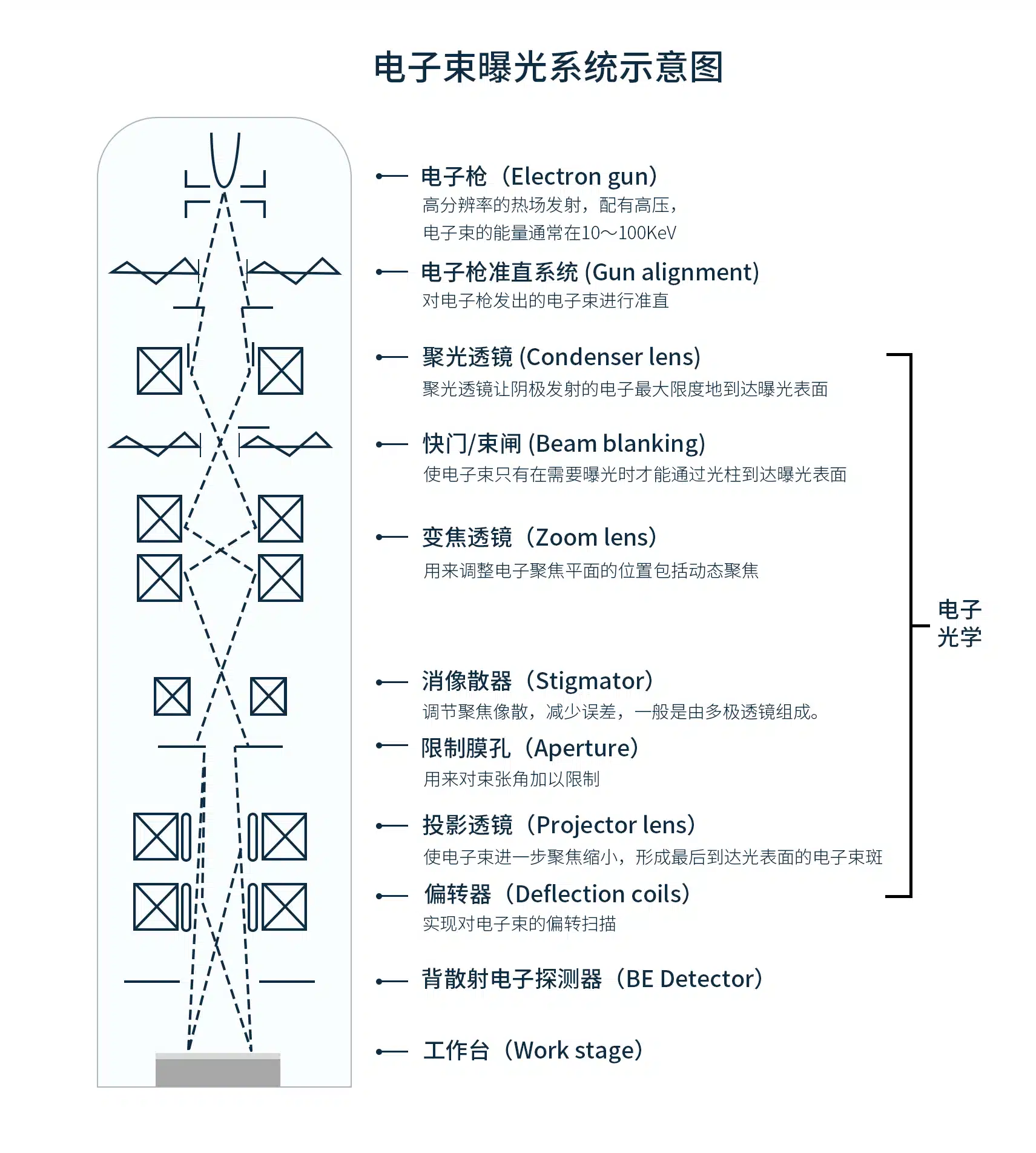
Important Indicators of Electron Beam Exposure Systems
Electron beam exposure systems have several important indicators, as follows:
Minimum Beam Diameter It directly affects the minimum size of the exposed pattern. To obtain a smaller spot diameter, the following measures can be adjusted: ① Set the highest possible accelerating voltage; ② Use a smaller aperture diameter; ③ Use a small working distance; ④ Set a small scanning field; ⑤ Set a small exposure step.
Accelerating Voltage Its value is generally between 10~100kv. The higher the accelerating voltage, the higher the resolution of the system, the smaller the proximity effect produced by the exposure, and the thicker the resist that can be exposed.
Electron Beam Current The larger the beam current, the faster the exposure speed, but the maximum exposure speed is limited by the scanning frequency, and a larger beam current will also correspond to a larger spot size.
Scanning Speed The faster the scanning speed, the faster the exposure speed, usually expressed in frequency (e.g., 50MHz).
Scanning Field Size If the scanning field is large, most of the exposure pattern can be exposed within the scanning field, thus avoiding errors caused by scanning field stitching.
In addition, indicators such as worktable movement accuracy, alignment accuracy, and field stitching accuracy are also important.
Classification of Electron Beam Exposure Methods
Electron beam exposure methods can be classified from different perspectives, as follows:
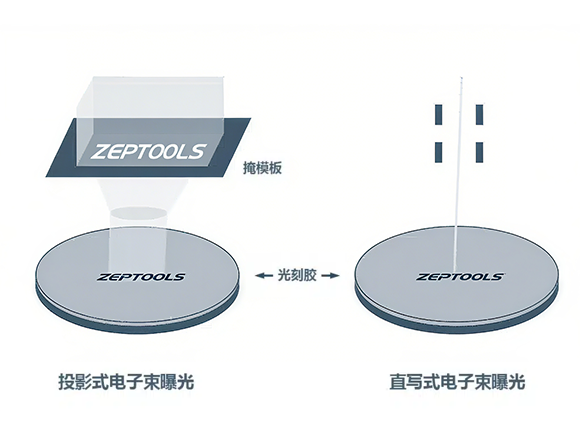
According to the working method, it can be divided into projection exposure and direct writing exposure. Projection exposure requires a mask, while direct writing exposure does not require a mask.
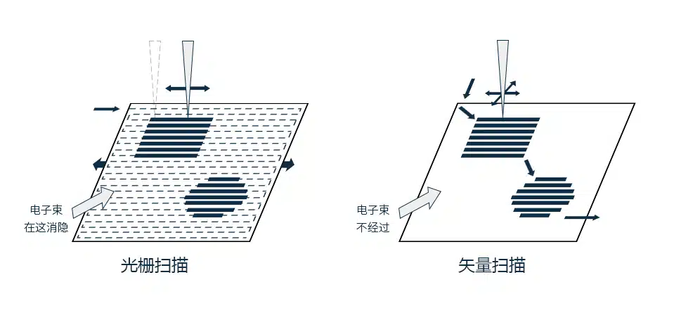
According to the scanning method, it can be divided into raster scan and vector scan. Raster scanning uses a Gaussian circular beam, and the electron beam continuously scans point by point in the entire scanning field. The pattern is exposed by controlling the on/off of the shutter (beam gate). Its advantages are simple control and no need to control the deflection system; however, the disadvantages are low production efficiency, and because the scanning field is relatively small, it must be combined with the movement of the workpiece stage to complete the exposure. The advantages of vector scanning are high exposure efficiency, scanning and exposure only in the graphic area, reducing the time spent by the lens in the non-graphic area, and a variable rectangular beam can be used; however, the disadvantage is that the control system is complex, because vector scanning must control the deflector, unlike raster scanning which uses a fixed deflection method.
According to the electron beam shape, it can be divided into Gaussian beam (circular beam) and shaped electron beam (rectangular beam). In vector scan mode, the exposure time of the pattern is related to the number of beam spot projections. In a fixed Gaussian beam (circular beam) spot mode, 24 projections are required.
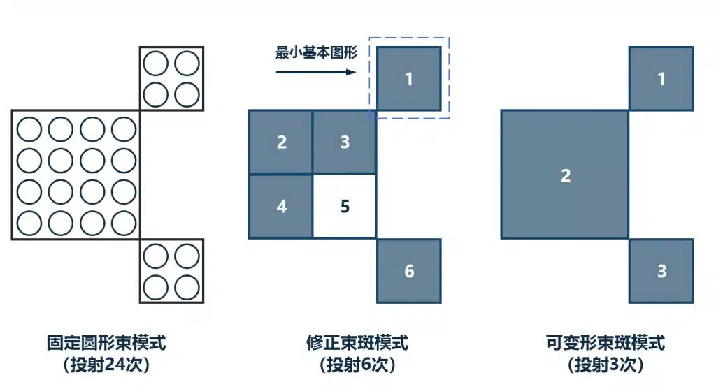
In order to speed up the exposure rate, the pattern can be decomposed into a combination of the smallest basic patterns, using the smallest basic pattern as the shape of the electron beam spot. In this modified spot mode, only 6 projections are needed. However, in actual production, the pattern is not immutable and needs to be frequently reset. Therefore, a more flexible projection method is needed. A variable spot mode can be applied to situations with diverse patterns. As shown in the figure below, in the variable spot mode, the electron beam spot can be adjusted according to the specific pattern, changing the basic shape of the spot, thereby reducing the number of projections to 3.
Introduction to Electron Beam Resist
Photoresist is a kind of etching-resistant thin film material. Under the irradiation or radiation of ultraviolet light, excimer laser, electron beam, ion beam, X-ray and other light sources, its solubility will change.
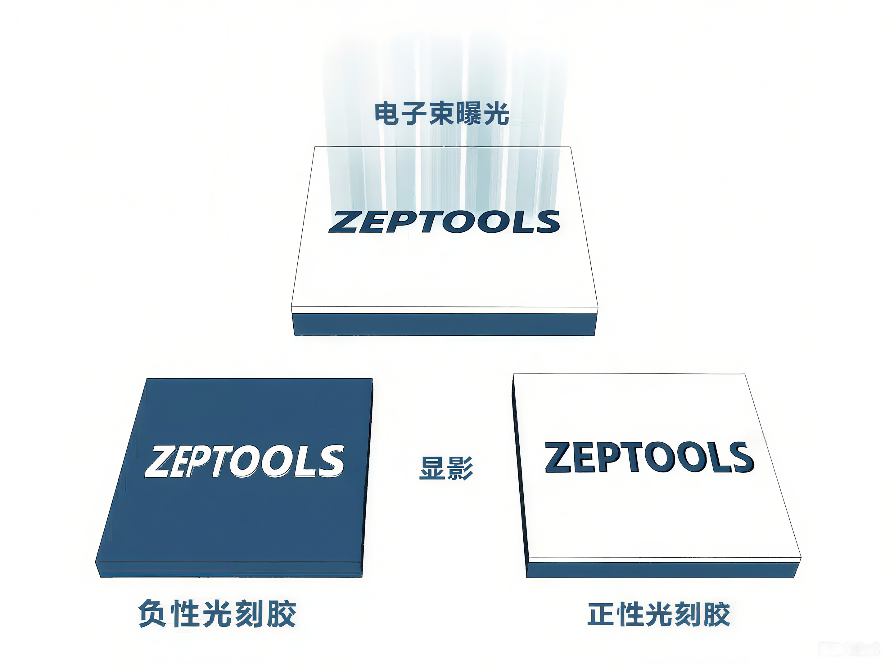
Electron beam resist is a type of photoresist, which is usually divided into positive resist and negative resist. The classification is based on which reaction, crosslinking reaction or chemical bond breakage, is dominant after the photoresist is irradiated. However, the positive and negative characteristics of photoresist are not absolute. For example, the electron beam positive resist PMMA, when irradiated with 10 times the normal exposure dose, the resin in the exposed area will be carbonized and will remain during development, at which time its characteristics can be used as a negative resist.
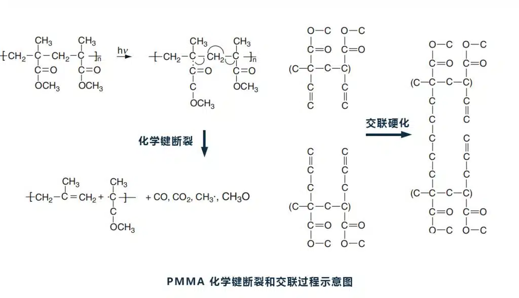
The characteristic of positive photoresist is that in the exposed area, the chemical bond breakage reaction is dominant, making the photoresist in this area easily soluble in the developer.
Negative photoresist is different. In the exposed area, the crosslinking reaction is dominant, and small molecules will form macromolecules through crosslinking polymerization, resulting in the photoresist in this area being difficult to dissolve in the developer.
Key Parameters of Photoresist
Similar to ultraviolet photoresist, when selecting or evaluating the application of a photoresist in a process, we usually refer to the following four key parameters: sensitivity, contrast, resolution, and etch resistance.
Sensitivity The higher the sensitivity of the photoresist, the smaller the required exposure dose (irradiation amount). Its sensitivity is affected by many factors, such as electron energy keV (or accelerating voltage kV), substrate material, process conditions, and developer used.
Contrast High-contrast photoresist can obtain steeper sidewalls, provide greater processing leeway, achieve better resolution and higher aspect ratio structures, and make it less sensitive to proximity effects, and the pattern density is also higher. Low-contrast photoresist is only suitable for 3D grayscale lithography.
Resolution This parameter defines the size of the smallest feature that can be obtained, or the minimum distance between two structures.
Etch Resistance If there is a need for etching in subsequent processes, a photoresist that can maintain its own complete characteristics during chemical (wet) etching and physical (dry) etching should be selected.
In addition, when selecting a suitable photoresist, it is also necessary to comprehensively consider parameters such as the positive and negative characteristics of the photoresist, process tolerance, adhesion, thermal flow, swelling effect, and shelf life.
Commonly Used Photoresists
Different photoresists need to be used for different application scenarios. This section mainly introduces several commonly used electron beam resists in experiments, including positive resists PMMA, ZEP-520A, AR-P 6200 (SCAR62), and negative resist HSQ.
PMMA (Positive Resist)
PMMA (poly-methyl methacrylate) is a high molecular polymer, also known as acrylic or plexiglass, and is currently the most widely used electron beam resist. By fully mixing 5%~10% PMMA powder with chlorobenzene or anisole (less toxic, concentration 2-4%), PMMA photoresist can be prepared.
It has the characteristics of being cheap, durable, and easy to operate, and it also has very high resolution and contrast, but low sensitivity and poor dry etching resistance (this characteristic is beneficial for lift-off processes, but not suitable for direct etching pattern transfer). Its sensitivity increases with decreasing relative molecular mass. Typical relative molecular masses of PMMA are 495 kg/mol and 950 kg/mol. In addition, the contrast and sensitivity can be controlled by changing the proportion of MIBK in the developer mixture (MIBK:IPA). Sensitivity increases with increasing MIBK proportion in the developer, while contrast decreases.
Zep-520A (Positive Resist)
ZEP-520A is a popular commercial photoresist developed by Nippon Zeon of Japan. It is a modified PMMA with a benzene ring, composed of a copolymer of α-chloromethacrylate and α-methylstyrene, often used as a PMMA alternative.
This photoresist has high resolution and high contrast, achieving graphic structures of 10-30nm, with resolution comparable to PMMA; it also has higher sensitivity (3-5 times higher) and higher dry etching resistance (more than 5 times higher than PMMA). However, it is expensive and has a one-year shelf life. For ultra-high resolution (sub-10nm) requirements, PMMA may be better. Furthermore, ZEP-520A is not easily removed after exposure, development, and hard bake, and ZDMAC is usually used for removal.
AR-P 6200 (CSAR62) (positive resist)
AR-P 6200 (CSAR62) has ultra-high resolution (<10nm) and high sensitivity, and the sensitivity can be controlled by selecting the appropriate developer. It also has high contrast (>15) and a high aspect ratio (up to 20:1).
It also has good process stability and dry etching resistance (twice that of PMMA); good adhesion to the substrate, and is not prone to delamination or cracking. However, it also has some drawbacks, such as low Young's modulus, making it prone to collapse, adhesion, and overturning; a low melting point, resulting in resist melting; and shrinkage on the surface of the pattern.
HSQ (negative resist)
HSQ is developed by Dow Corning. Its composition is based on an inorganic compound of silicon dioxide, consisting of hydrogen silsesquioxane (HSQ) resin in a polar solvent of methylisobutylketone (MIBK).
HSQ has extremely high resolution (<10nm), but low sensitivity and long exposure times. It is developed through a chemical reaction (unexposed HSQ reacts with a diluted NH4OH or NaOH developer to produce H2), rather than dissolution development, resulting in good process stability after development. In addition, it has good observation performance under an electron microscope, does not require gold plating, and is an excellent etching mask material for silicon.
However, HSQ has a short shelf life of only 6 months, while powdered HSQ (H-SiOx) has a longer shelf life. Its storage conditions are also demanding; the colloid is easily oxidized when exposed to air, resulting in gel solidification, and needs to be stored sealed at low temperatures (5℃). At the same time, it has extremely high contrast, making it easy to prepare high aspect ratio structures with steep profiles. It is a stretchable photoresist, and the edges of the lines after development are vertical, with good adhesion and toughness, and are not easily broken.
Proximity Effect
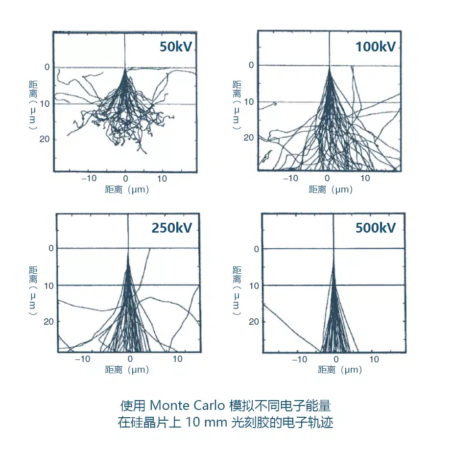
The proximity effect in electron beam lithography refers to the scattering of electrons in the photoresist and substrate when two exposed patterns are close together, causing the electrons to deviate from their original incident direction. This can cause unexposed areas to be exposed, while some areas that should be exposed do not receive sufficient exposure, ultimately causing distortion of the exposed pattern, resulting in reduced contrast and resolution.
Correction Methods
There are three main methods for correcting the proximity effect: ① Dose correction; ② Pattern size compensation; ③ Background exposure compensation.
Dose Correction This is the most widely used and effective method. Its principle is to artificially control the exposure energy so that all exposed patterns receive uniform and consistent exposure energy. Dose correction can be divided into self-consistent technology (physical correction) and geometric pattern cutting. Self-consistent technology (physical correction) provides more accurate correction results, but the computational cost is high for large-scale integrated circuit design; the exposure dose distribution calculated by the geometric pattern cutting method is relatively rough, but the calculation speed is very fast.
Pattern Size Compensation This method compensates for the effects of locally high or low energy by reducing or increasing the size of each pattern. This method is suitable for simple and periodically repeating patterns.
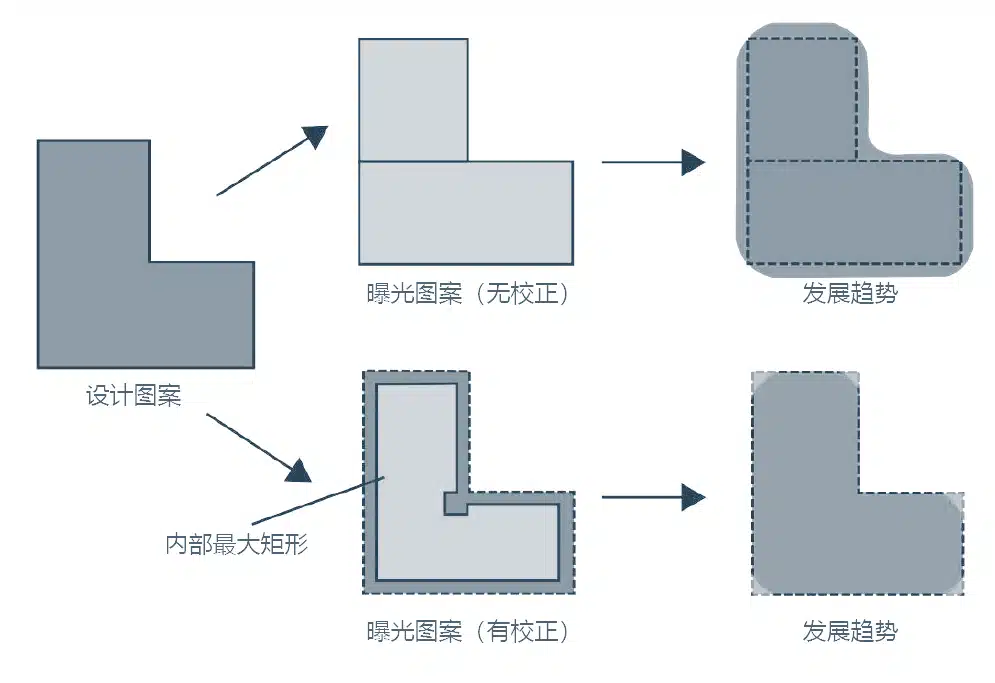
Background Exposure Compensation This method uses the superposition of secondary exposure energy to achieve a balanced energy distribution in each area. This method does not require calculation of the energy distribution, but may reduce the contrast of the exposed pattern. It is suitable for raster scanning exposure systems.
In addition, the simplest and most effective way to reduce the proximity effect is to increase the electron beam energy and reduce the electron beam resist thickness, but it is necessary to consider that high electron beam energy may damage the substrate and cause overheating.
Application Cases
Related News

Contact Us
Mobile Phone: 15756003283
Email: support@zeptools.com、micage@zeptools.com
Address: No.15, Electronic Venture Park, Dongshi, Tongling City, Anhui Province, China