



ZEPTOOLS Technology | How does electron beam lithography achieve nanometer-scale resolution?
Release time:
2025-08-08
In the fields of semiconductor manufacturing and micro-nano processing, "nanometer-scale resolution" is a core indicator for measuring technological advancement—it determines the density of transistors on a chip, the precision of quantum devices, and even impacts breakthroughs in cutting-edge fields such as photonic crystals and two-dimensional materials.
In the fields of semiconductor manufacturing and micro-nano processing, "nanometer-scale resolution" is a core indicator of technological advancement—it determines the density of transistors on a chip, the precision of quantum devices, and even influences breakthroughs in cutting-edge fields such as photonic crystals and two-dimensional materials. As the only key technology currently capable of achieving "from 0 to 1" nanometer manufacturing, electron beam lithography (EBL), with its ability to break the optical diffraction limit, has become a "must-have" for global scientific research and industry. This article will analyze how electron beam lithography achieves nanometer-scale resolution, from its technical principles and core support to its practical applications, and will highlight the innovative breakthroughs of ZEPTOOLS Technology in this field.
I. Theoretical Foundation: Short Electron Wavelength, Breaking the Optical Diffraction Limit
To understand the nanometer-scale resolution of electron beam lithography, it is first necessary to compare its essential differences from optical lithography. Optical lithography is limited by the Rayleigh criterion

(K is a constant, λ is the wavelength of light, and NA is the numerical aperture), and its resolution is limited by the diffraction effect of light—even with extreme ultraviolet (EUV) lithography (wavelength 13.5 nm), multiple exposures are still required to achieve a 7 nm process.
The core advantages of electron beam lithography are: The de Broglie wavelength of electrons is much shorter than that of visible light .
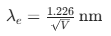
(V is the accelerating voltage, in kV), the electron wavelength shortens exponentially as the accelerating voltage increases. For example:
When the accelerating voltage is 100 kV, the electron wavelength is only 0.12 nm (approximately 1/5000 of optical ultraviolet light);
Even at low voltages (such as 1 kV), the wavelength can still reach 0.39 nm, which is far lower than the wavelength of optical lithography (such as 193 nm for deep ultraviolet DUV).
This extremely short wavelength theoretically allows electron beams to achieve atomic-scale resolution (such as a single atom diameter of approximately 0.1 nm), providing the physical basis for nanometer-scale processing.
II. Technical Support: "Full-Chain High-Precision Technology" from Electron Gun to Sample Stage
Theoretical advantages must be translated into actual resolution through the synergistic optimization of hardware and software. As a leading domestic enterprise in electron beam lithography equipment, ZEPTOOLS Technology has built a full-chain high-precision control system "from electron emission to pattern formation" through independent research and development of core components and intelligent systems, specifically reflected in the following four aspects:
1. Field Emission Electron Gun: A "Nanometer-Scale Brush" with High Brightness and Low Divergence
The quality of the electron beam directly affects the resolution, and the electron gun is the core component that determines the quality of the electron beam. The flagship model ZEL304G of ZEPTOOLS Technology uses a Schottky field emission electron gun , which has higher electron beam brightness (beam current density > 5300 A/cm²) and a smaller divergence angle (beam spot diameter ≤ 2 nm after focusing with a condenser lens) compared to traditional thermionic emission electron guns, ensuring that the electron beam can accurately "draw" nanometer-scale lines.
2. Laser Interferometer Sample Stage: A "Nanometer-Scale Ruler" with Sub-Nanometer Positioning
In micro-nano processing, sample positioning errors will directly lead to pattern distortion. The ZEL304G is equipped with a high-precision laser interferometer sample stage , with a travel range of 105 mm × 105 mm. It uses laser interferometry to monitor the sample position in real time, with a positioning accuracy of up to sub-nanometer level. This configuration supports high-precision stitching with a large travel range (such as seamless stitching of long gratings) and multi-layer overlay (calibrating the position using a two-point calibration function, error < 0.1 μm), meeting the high-precision preparation requirements of complex micro-nano structures.
3. High-Performance Pattern Generator: A "Nanometer-Scale Brush" with High-Speed Scanning and Super-Resolution
The pattern generator is the "brain" that controls the scanning path of the electron beam. ZEPTOOLS Technology uses a 20-bit D/A converter and a 50 MHz high-speed scanning module , supporting various vector scanning modes such as sequential scanning (Z-type), cyclic scanning (S-type), and spiral scanning. Its maximum scanning speed reaches 50 MHz, and with the FPGA control core, it achieves ultra-high image resolution of ≤ 1 nm @ 15 kV (at 15 kV accelerating voltage) while ensuring ultra-high-speed scanning, with a minimum single-exposure linewidth of only 2 nm.
4. Proximity Effect Correction: Software-Driven "Nanometer-Scale Error Correction"
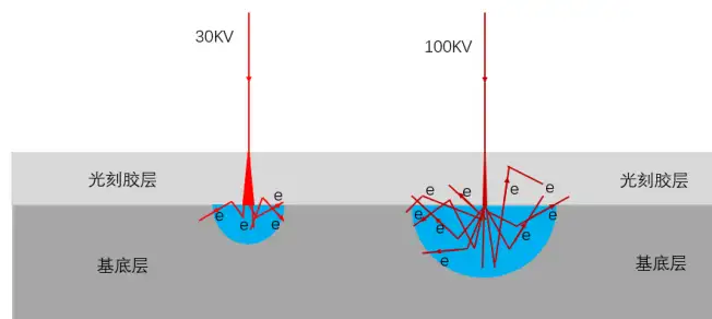
Electron beams in photoresist will undergo forward scattering (beam spot expansion) and backscattering (secondary effects), leading to overlapping exposure in adjacent areas, forming a "proximity effect" that directly reduces resolution. ZEPTOOLS Technology uses a built-in proximity effect correction function , based on a double Gaussian distribution model

to simulate the electron energy deposition distribution and dynamically adjust the exposure dose in different areas (such as increasing the dose in underexposed areas and reducing the dose in overexposed areas), ultimately achieving a corrected linewidth error of < 5%. Taking the ZEL304G as an example, its dose correction function can control the actual exposure result error of a 200 nm design linewidth trench within ± 10 nm, significantly improving the uniformity of nanometer-scale patterns.
III. Application Verification: "Nanometer-Scale Breakthrough" from Laboratory to Industrialization
The technical strength of ZEPTOOLS Technology's electron beam lithography machines has been fully verified in scientific research and industrial applications:
Scientific Research Field : Supports the preparation of two-dimensional material (such as graphene, MoS₂) devices. Through technologies such as 0.38 nm linewidth testing (minimum single-exposure linewidth) and seamless stitching of long gratings (304 nm period), it assists in breakthroughs in basic research such as quantum tunneling devices and three-dimensional metasurfaces.
Industrial Field : Provides high-precision processing solutions for microelectromechanical systems (MEMS), photomask manufacturing, etc. For example, its PMMA/HSQ resist compatibility (supports thick resist testing) can meet the mass production needs of customized devices such as high-frequency devices and sensors.
Domestic Breakthrough : In 2024, ZEPTOOLS Technology's ZEL304G achieved mass production, with a domestication rate of over 95%. Key performance indicators (such as resolution and overlay accuracy) have reached the level of mainstream international equipment (such as Raith150 Two, Vistec SB3050), breaking the long-term monopoly of the United States and Japan in the field of high-end electron beam lithography.
Conclusion: ZEPTOOLS Technology—the "China Engine" of Nano-Manufacturing
From theoretical breakthroughs to technological implementation, the nanometer-level resolution of electron beam lithography is the result of ZEPTOOLS Technology's decade-long dedication to technological development: from the independent research and development of field emission electron guns, to the precision breakthrough of laser interference sample stages, and to the algorithm optimization of proximity effect correction, every step marks the innovative height of "Made in China."
In the future, as ZEPTOOLS Technology continues to advance the research and development of new technologies such as multi-beam parallel and hybrid lithography, electron beam lithography will further break through the balance bottleneck of "high precision and high efficiency," providing a more powerful "nanometer-level manufacturing engine" for cutting-edge fields such as quantum computing and two-dimensional materials.
Related News

Contact Us
Mobile Phone: 15756003283
Email: support@zeptools.com、micage@zeptools.com
Address: No.15, Electronic Venture Park, Dongshi, Tongling City, Anhui Province, China