



ZEPTOOLS Technology | What are the core differences between maskless lithography and traditional mask lithography? In what scenarios is maskless lithography more suitable?
Release time:
2025-08-11
In semiconductor manufacturing and micro-nano fabrication, lithography is a key process determining the performance of chips and the precision of micro-nano structures. Maskless lithography and traditional mask lithography have significant differences in their core principles and technical characteristics, which determine their respective applications.
In semiconductor manufacturing and micro-nano fabrication, lithography is a crucial step that determines the performance of chips and the precision of micro-nano structures. Maskless lithography and traditional mask lithography have significant differences in their core principles and technical characteristics, which determine their respective applications.
The essential difference between maskless lithography and traditional mask lithography lies in the method of pattern generation :
1. Traditional Mask Lithography : Relies on physical masks; expensive metal or glass masks need to be pre-fabricated. Once the pattern is solidified, it cannot be modified. Suitable for mass production and standardized production.
2.ZEPTOOLS DMD Maskless Lithography :
Dynamic Pattern Generation : Projects patterns in real-time using a Digital Micromirror Device (DMD), eliminating the need for physical masks. Design modifications take effect immediately.
High Flexibility : Supports 2D/3D grayscale lithography, stitching, and in-situ drawing, adapting to complex micro-structure processing needs.
Cost and Cycle Advantages : Eliminates mask fabrication costs, resulting in low per-exposure costs. Suitable for research and development and small-batch production.
Applicable Scenarios: Precisely Matching Diverse Needs
Maskless lithography technology, with its flexibility and high precision, demonstrates significant advantages in the following areas:
1. Scientific Research and Prototype Development
2D Material Devices : Such as MoS₂/WSe₂ heterojunction photodetectors and graphene electrode preparation, requiring rapid iteration of pattern design.
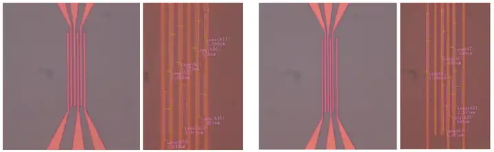
MEMS and Microfluidics :ZEPTOOLS lithography machines support a minimum linewidth of 0.5μm and overlay accuracy of ±0.5μm, meeting the complex structural processing requirements of miniature sensors and microvalves.
Nanoimprint Templates : 3D structures such as Fresnel lenses are achieved through grayscale lithography and applied to AR/VR optical devices.
2. Rapid Prototyping and Small-Batch Production
Photodetector R&D : Such as tellurium nanogrid electrodes and PdSe₂ differential pressure sensors, using maskless lithography to accelerate material verification and process optimization.
Customized Electronic Devices : Supports importing DXF and GDS format files, adapting to different sizes of silicon wafers (4/8 inches), meeting the flexible needs of laboratories and startups.
3. High Precision and Special Process Scenarios
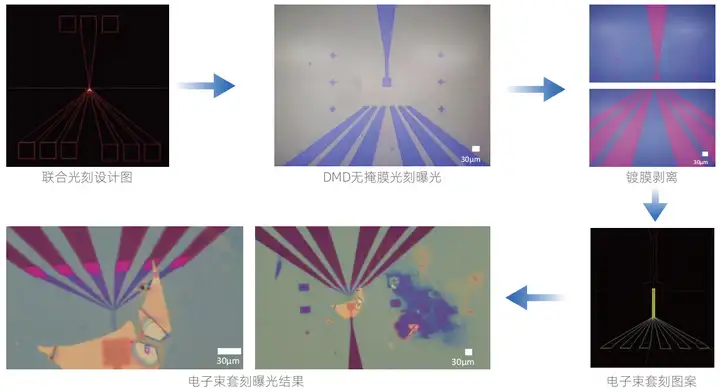
Electron Beam Combined with Lithography : Combining DMD ultraviolet lithography and electron beam overlay to achieve 30μm high-resolution pattern superposition.
Silicon-Based Heterojunction Integration : Optimizes graphic quality through OPC correction algorithms to improve the yield of Si/PbSe and other heterojunction devices.
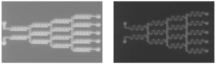
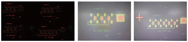
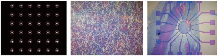
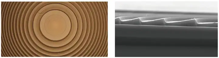
ZeptoTools DML Series: Domestic Solutions Empowering Micro-Nano Manufacturing
Relying on its independently developed DMD maskless lithography technology,ZEPTOOLS has launched the ZML series of equipment, with core advantages including:
High Precision and Stability : Equipped with a 7.56μm pixel DMD chip, supporting a minimum feature size of 0.5μm and a repeat positioning accuracy of ±0.25μm.
Intelligent Operation : Features such as CCD autofocus, image binding, and stitching accuracy correction reduce the operational threshold.
Multi-Scenario Adaptability : Covering semiconductors, materials science, and biomedicine, from MEMS pressure sensors to artificial retina photodetectors.
Conclusion
Maskless lithography technology, with its flexibility, low cost, and high efficiency, is reshaping the landscape of micro-nano manufacturing.ZEPTOOLS, with the core technological advantages of its DML series products, provides a complete solution for research institutions and enterprises from prototype development to small-batch production. Whether it is 2D material innovation, MEMS device development, or customized electronic device production,ZEPTOOLS maskless lithography machines are the ideal choice for accelerating technological implementation.
Inquire Now :www.zeptools.cn | Technical Support: support@zeptools.com
Keywords : Maskless lithography, DMD technology, MEMS manufacturing, 2D materials, photodetectors,ZEPTOOLS, domestic lithography equipment
ZeptoTools DMD Maskless Lithography Machine
Related News

Contact Us
Mobile Phone: 15756003283
Email: support@zeptools.com、micage@zeptools.com
Address: No.15, Electronic Venture Park, Dongshi, Tongling City, Anhui Province, China