

Home
Products
SEM
Lithography System
In-situ TEM Holder
Stylus Profiler
Nanopositioning Stage
More...
Applications
About
Contact Us
Language
中文简体
English
Russian
News
ZEPTOOLS
Application Case
Frontier Information
Knowledge
The Role of In Situ TEM Holders in Advanced Microscopy Techniques
The Role of In Situ TEM Holders in Advanced Microscopy Techniques Introduction to In Situ TEM Holders In the realm of advanced microscopy techniques, **in situ Transmission Electron Microscopy (TEM)** holders play a pivotal role in enhancing our understanding of materials at the atomic level. Unlike traditional microscopy, where samples are analyzed under static conditions, in situ TEM holders all
26
2026
/
06
Unlocking Precision: The Essential Role of Step Profilers in Electronic Measurement
Step profilers are critical instruments widely utilized in the electronic measurement sector, particularly for applications that demand high precision and accuracy. These specialized devices excel in measuring surface topography, enabling users to obtain detailed insights into the physical characteristics of various materials. This article aims to elucidate the functionalities and advantages of st
23
Advanced Functional Materials | ZEPTOOLS In-Situ TEM Enables Real-Time Electrical Monitoring of Plastic Deformation in Tungsten Nanowires
With the continued miniaturization of micro/nanoelectromechanical systems and advanced interconnect devices, the structural stability and functional reliability of metallic nanomaterials under extreme conditions face increasingly severe challenges. In these micro/nanodevices, the stresses experienced by materials can easily exceed their yield strength, triggering irreversible plastic deformation. Even extremely small plastic strains can induce the initiation and propagation of fatigue cracks, ultimately leading to catastrophic functional failure of the device. Therefore, achieving early identification and accurate assessment of plastic deformation at the micro/nano scale is of vital importance for predicting material failure and ensuring the operational safety of systems. Although electrical impedance changes, as a non-destructive and sensitive parameter, have been widely used for structural damage monitoring at the macroscale, their application in the field of micro/nanodevices remains difficult.
china electron beam lithography system
The Electron Beam Lithography system has evolved beyond pure research into a production‑ready tool for advanced semiconductor packaging, compound semiconductor devices,
22
China DMD maskless lithography machine
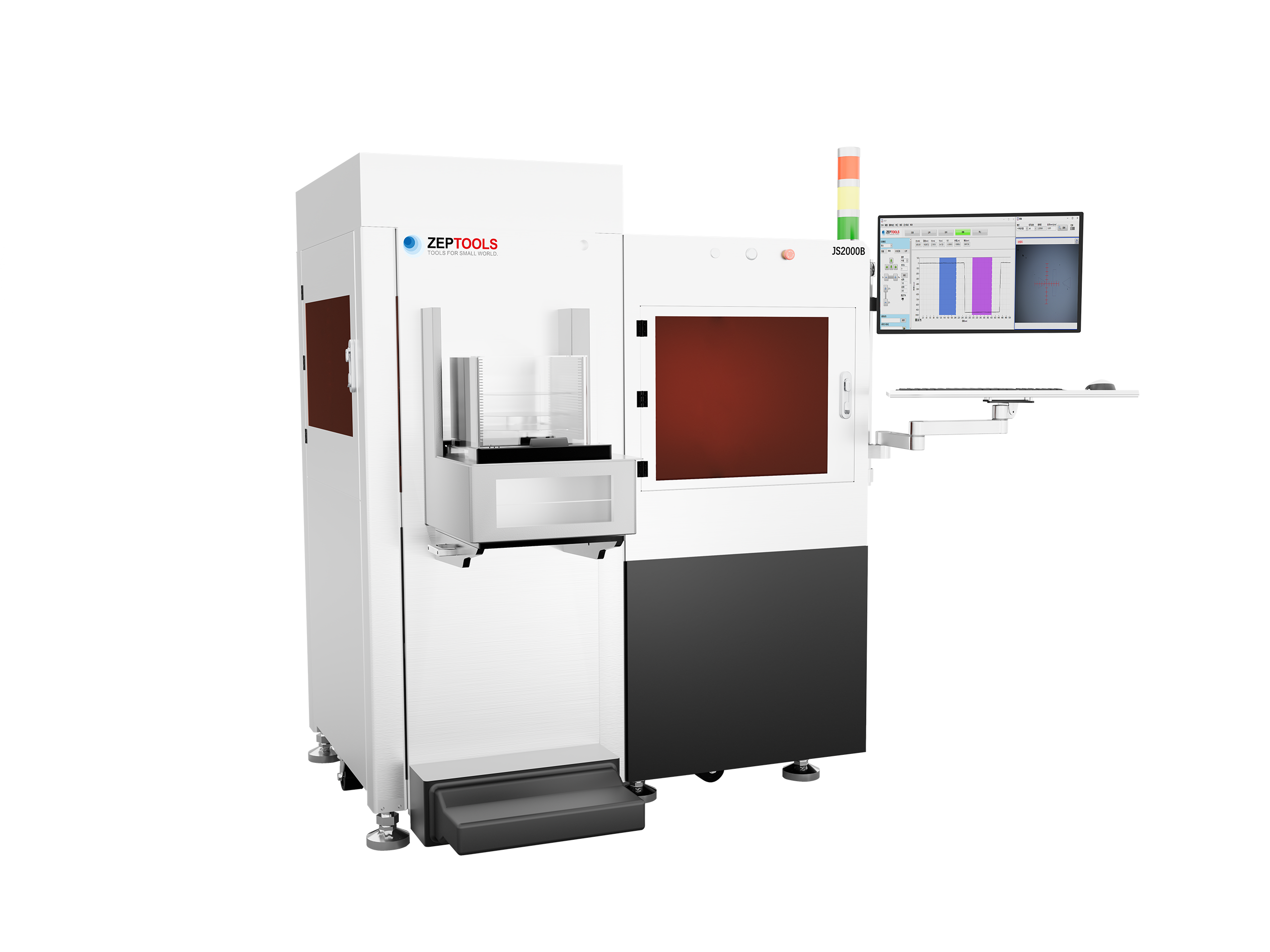
Engineered for high-mix manufacturing environments, the DMD maskless lithography machine redefines productivity by merging digital agility with industrial-grade robustness. This system employs a state-of-the-art DMD array with over 2 million individually addressable mirrors
Desktop Scanning Electron Microscopes: Revolutionizing Quality Control Processes
Desktop Scanning Electron Microscopes: Revolutionizing Quality Control Processes Table of Contents 1. Introduction to Desktop Scanning Electron Microscopes 2. What is a Desktop Scanning Electron Microscope? 3. The Technology Behind Desktop Scanning Electron Microscopes 4. Advantages of Desktop Scanning Electron Microscopes in Quality Control 5. Applications of Desktop Scanning Electron
20