



Product classification

Scanning Tunneling Microscope
Scanning Tunneling Microscope
Classification:
Product Description
Scanning Probe Microscopy
Scanning Tunneling Microscope
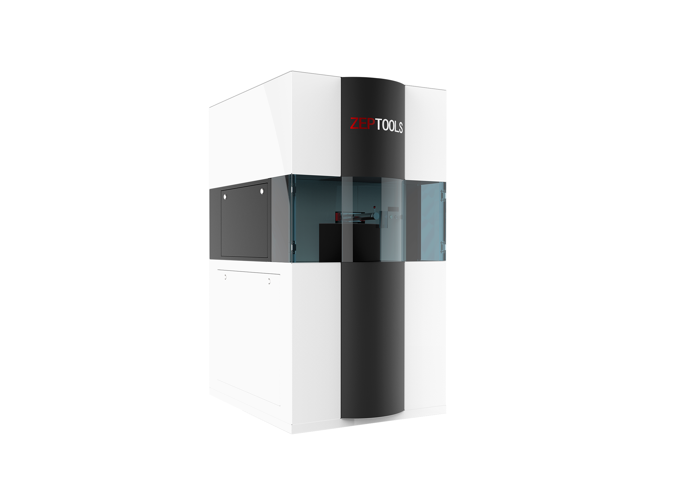
ULTRASCAN LT-100 Ultra-High Vacuum Scanning Tunneling Microscope
Atomic-scale studies of surface-related physical and chemical phenomena
Room temperature / 77K / 4K multi-temperature zones | Atomic-scale resolution | Ultimate vacuum 5×10⁻¹⁰ mbar
Scanning Tunneling Microscope (STM) is a core tool in surface science research, capable of imaging and performing spectroscopic measurements on material surfaces at the atomic scale. It is widely used in frontier fields such as surface physics research, low-dimensional materials, and the atomic structures and local electronic states of single molecules and thin films.
ZEPTOOLS ULTRASCAN LT-100 is built on ultra-high vacuum and double-layer liquid helium cryogenic technology. It is equipped with a sample preparation chamber, a load-lock chamber, and a multi-stage ultra-high vacuum pump set, enabling stable long-term observation at room temperature, liquid nitrogen temperature, and liquid helium temperature. It is available in multiple configurations, including the standard version, the TERS tip-enhanced Raman spectroscopy hybrid version, and MINI-STM, and supports customization on demand.
Main Technical Specifications
Ultra-high vacuum and liquid helium low temperature, providing stable support for atomic-scale observation
Product Model: ULTRASCAN LT-100
Operating Temperature Zones: Room temperature / Liquid nitrogen 77K / Liquid helium 4K
Ultimate Vacuum: Better than 5×10⁻¹⁰ mbar
Resolution: Atomic-scale resolution
Noise: Electronic noise < 500 fA, mechanical noise < 1 pm
Scan Range: Room temperature 3×3 μm; 77K 1×1 μm; 4K 0.6×0.6 μm
Application Cases
Measured imaging results of ULTRASCAN LT-100 in frontier surface science research
 Monolayer and bilayer borophene on Cu(111) surface |  Moiré superlattice of monolayer FeO(111) film on Au(111) |
 Monolayer borophene on Ag(100) surface |  Honeycomb structure of Sn-Bi overlayer on Si(111) surface |
 STM image of coexisting α and β phases of two-dimensional CO on Cu(111) surface at 77K |  Two-dimensional borophene sheets on Ag(111) surface |
 Honeycomb structure of Sn-Bi overlayer on Si(111) surface |  Adsorption of 0.01 monolayer H₂S molecules on Au(111) surface |
Selected Customers
Trusted by numerous universities, research institutions, and enterprises

Start Your Journey of Atomic-Scale Observation
Independently developed by ZEPTOOLS, safeguarding frontier scientific research
Recommended Products


Welcome your message consultation

Contact Us
Mobile Phone: 15756003283
Email: support@zeptools.com、micage@zeptools.com
Address: No.15, Electronic Venture Park, Dongshi, Tongling City, Anhui Province, China