



Product classification

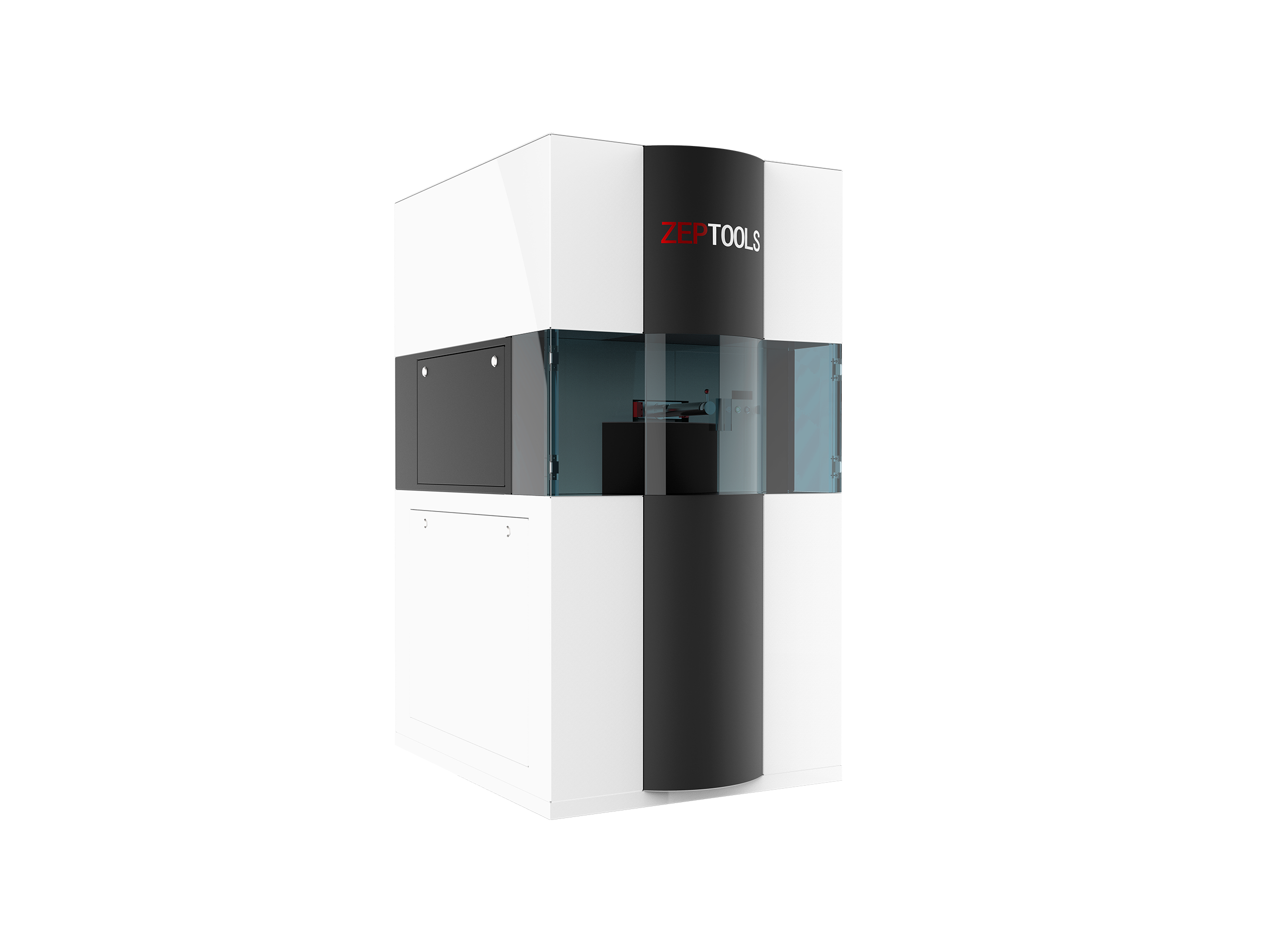
ZEM Ultra Field Emission SEM
ZEM Ultra Field Emission Scanning Electron Microscope
Classification:
Product Description
Schottky Field Emission Scanning Electron Microscope
ZEM Ultra
Schottky Field Emission Electron Source
The Pinnacle of Scanning Electron Microscope Performance
Better than 2.5nm Resolution | 1,000,000x Magnification
Ultimate Resolution, Pinnacle of Micro-Nano
Breaking the Performance Boundaries of Equipment
The ZEM Ultra Field Emission SEM is designed for advanced microstructure observation and high-precision material analysis, providing researchers with detailed imaging performance and reliable operation. As a high-resolution scanning electron microscope, it uses advanced field emission technology to achieve clear surface observation and support research in semiconductors, materials science, microelectronics, nanotechnology, and other scientific fields. The system helps users analyze material characteristics and explore microscopic structures with greater accuracy.
Built with precision engineering and careful manufacturing processes, the ZEM Ultra Field Emission SEM focuses on stability, flexibility, and long-term performance. From key component assembly and system integration to calibration and quality testing, each production stage is controlled to ensure dependable operation. With advanced imaging capabilities and user-oriented design, the system provides an effective solution for laboratories and research teams requiring accurate micro-scale analysis and innovative material exploration.
The ZEM Ultra Scanning Electron Microscope adopts an advanced Schottky Field Emission Electron Source, combined with a unique three-stage independent vacuum design. This design ensures a resolution better than 2.5nm, perfectly meeting the characterization needs of most samples' micro-nano structures.
Not just clarity. The ZEM Ultra comes standard with a large beam current and an extra-large sample chamber, laying the foundation for its powerful expandability. It supports integration of in-situ functional sample stages and high-end analytical accessories such as EDS and EBSD, making it an all-around flagship platform for scientific research and industrial inspection.
ZEM Series Scanning Electron Microscopes
Full Series Coverage, Choose Your Preferred ZEPTOOLS SEM
| Product Model | ZEM Ultra | ZEM30 Pro | ZEM30 | ZEM20 Pro | ZEM20 | ZEM18 | ZEM10 |
| Resolution | <2.5nm | 2.5nm | 3nm | 3nm | 4nm | <6nm | <10nm |
| Maximum Magnification | 1,000,000x | 500,000x | 500,000x | 500,000x | 360,000x | 360,000x | 250,000x |
| Electron Gun | Schottky Field Emission | LaB6 | Tungsten Filament | LaB6 | Tungsten Filament | Tungsten Filament | Tungsten Filament |
| Accelerating Voltage | 1-15kV Continuously Adjustable | 3-30kV Continuously Adjustable | 3-30kV Continuously Adjustable | 3-20kV Continuously Adjustable (Upgradeable to 30kV) | 3-20kV Continuously Adjustable (Upgradeable to 30kV) | 3-20kV Continuously Adjustable | 5kV/10kV/15kV |
| Detector Type | SE BSE EDS (Optional) | SE BSE EDS (Optional) | SE BSE EDS (Optional) | SE BSE EDS (Optional) | SE BSE EDS (Optional) | SE BSE EDS (Optional) | SE or BSE |
| In-Situ Expansion Capability | Yes | Yes | Yes | Yes | Yes | Yes | —— |
Application Cases
Exceptional Imaging Technology Meets All Your Requirements

More Cases
ZEPTOOLS ZEM Series SEM Helps Research Teams Publish High-Level Journal Achievements


Some Customers
The Trusted Choice of Numerous Universities, Research Institutions, and Enterprises

Start Your High-Resolution Observation Journey
Independently Developed by ZEPTOOLS, Providing a Complete Set of Micro-Nano Analysis Solutions
Recommended Products

Welcome your message consultation

Contact Us
Mobile Phone: 15756003283
Email: support@zeptools.com、micage@zeptools.com
Address: No.15, Electronic Venture Park, Dongshi, Tongling City, Anhui Province, China