



Product classification

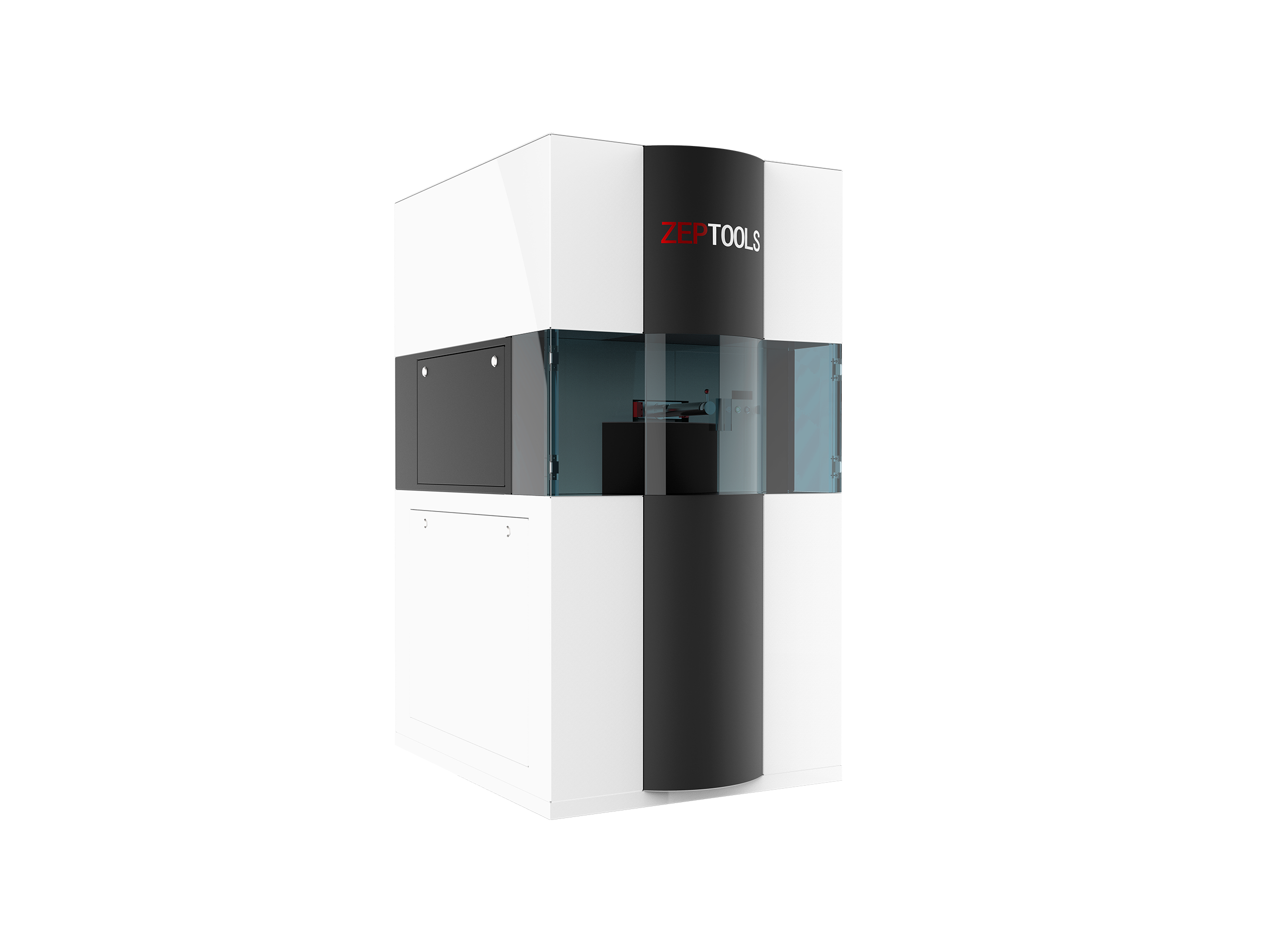
DMD Maskless Lithography System
DMD Maskless Lithography System
Classification:
Product Description
DMD Maskless Lithography
ZML Series Maskless Lithography System
Diverse Models
High Efficiency, Flexibility, High Resolution, and High Overlay Accuracy
Critical Dimension 0.5μm | High-Precision Stepper Lithography
ZEPTOOLS ZML Series DMD Maskless Lithography System adopts advanced digital micromirror direct-write technology, enabling precise exposure of arbitrary micro/nano patterns without the need for traditional masks, with excellent processing accuracy and stable imaging. The system features a compact design, combined with intelligent autofocus and an intuitive operating system, making it easy to learn and efficient to use. It can significantly shorten R&D cycles and reduce mask-making costs. It is widely suitable for microfluidics, MEMS, functional thin films, 2D material devices, and other scenarios, making it an ideal micro/nano fabrication system for laboratories and small-batch trial production that balances high precision, high flexibility, and high cost-effectiveness.

Main Technical Specifications
Full series coverage — choose the maskless lithography system you prefer
| Product Model | ZML10A | ZML100A | ZML200A |
| Minimum Critical Dimension | Submicron-Scale Pattern Fabrication | Submicron-Scale Pattern Fabrication | High-Precision Submicron-Scale Pattern Fabrication |
| Overlay Accuracy | Meets Basic Micro/Nano Fabrication Requirements | Meets Precision Micro/Nano Fabrication Requirements | Meets Precision Micro/Nano Fabrication Requirements |
| Focusing Method | Image Autofocus | Laser Active Focusing | Laser Active Focusing |
| Rotation Stage | Manual Rotation Stage | Motorized Rotation Stage | Motorized Rotation Stage |
| Data Format | DXF, GDS, BMP | DXF, GDS, BMP | DXF, GDS, BMP |
Application Cases
Exceptional lithography technology to meet your various requirements

2D Material Lithography Electrodes (left), Photodetectors (right)

20mm×20mm Semiconductor Device, Four-Layer Overlay, Minimum Linewidth 6μm

Microfluidic Chip (left), Microfluidic Master Mold (right)

DMD UV Lithography Achieves Overlay Function

Overlay Electrodes After Tellurium Nanomesh Etching

Grayscale Lithography Fresnel Lens [3D grayscale lithography to realize Fresnel lens; the SEM cross-sectional image shows continuous step variation]

Combined DMD UV and Electron Beam Lithography [Models used: ZML10A and ZEL304G]
More Cases
ZEPTOOLS DMD Maskless Lithography Systems Help Research Teams Publish High-Level Journal Results


Selected Customers
The trusted choice of numerous universities, research institutions, and enterprises

Start Your Micro/Nano Lithography Journey
Independently developed by ZEPTOOLS, providing a complete set of micro/nano analysis solutions
Recommended Products

Welcome your message consultation

Contact Us
Mobile Phone: 15756003283
Email: support@zeptools.com、micage@zeptools.com
Address: No.15, Electronic Venture Park, Dongshi, Tongling City, Anhui Province, China